In early 2018, Nvidia showcased real-time ray tracing using their DGX Station supercomputer and the DXR API. The Turing architecture introduced in late 2018 had significant improvements enabling real-time ray tracing. The RTX AIBs featured fixed-function RT inference cores for ray-tracing acceleration. Nvidia also introduced DLSS, leveraging AI to improve gaming performance. Turing GPUs incorporated tensor cores for matrix math processing. Texture Space Shading allowed for efficient caching and sampling of shading results. The Turing architecture laid the foundation for dedicated ray tracing and tensor engines, full mesh-shading capabilities, and advancements in real-time rendering. Nvidia’s DLSS 3.0 further improved performance, enabling 4K real-time ray tracing at respectable frame rates.
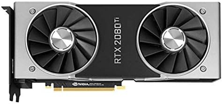
In early 2018, Nvidia demonstrated real-time ray tracing at GDC and again at GTC using their DGX Station supercomputer through the DXR API. The $50,000 DGX contained four NVLink four-way interconnected Nvidia Tesla V100 add-in boards (AIBs), each with a 5,120-shader Volta GPU running at 1.46GHz with 16GB of HMB2 local memory, and capable of 7 TFLOPS double-precision, for a total of 40,960 shaders and 128GB of memory. Also, there was a 2.2Hz 20-core Intel Xeon E5-2698 v4 Broadwell-EP processor with 256 B DDR4 that could produce 800 GFLOPS, which in total provides a theoretical compute capability of 28.8 TFLOPS. I calculated the MIPS and FLOPS necessary to do that and, based on Moore’s law, predicted we would have real-time ray tracing with a single GPU in less than six years.[i] Later that year at Siggraph 2018, Nvidia surprised everyone, including themselves, and showed real-time ray tracing running on a single chip—the Ray Tracing Texel eXtreme (RTX) Turing TU102 GPU on the RTX 2080 AIB. The industry had a new acronym—RTRT.
Ray tracing is a complex process of generating light rays that illuminate a visible scene, combined with the bounces and reflections of those visible rays. Millions, if not billions, of rays are generated, and their luminosity and color must be calculated for every instance of interaction they experience—it is a horrendous calculation workload and is aggravated by resolution because the number of visible pixels goes up as the product of X×Y.
Nvidia introduced their GeForce RTX and Quadro RTX AIBs at Siggraph in Vancouver, BC, in August 2018.
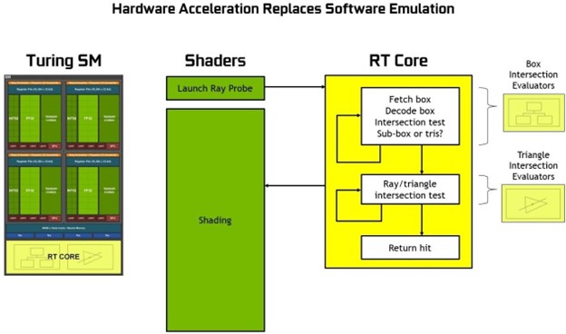
The RTX AIBs featured fixed-function RT inference cores designed to accelerate the operations needed to simulate rays, such as bounding volume hierarchy (BVH) traversal.
In the context of geometric objects, a bounding volume hierarchy (BVH) is a tree structure utilized to organize and categorize the objects. The objects themselves serve as the nodes or leaves of the tree, and they are enveloped by bounding volumes. These nodes are further organized into smaller sets and enclosed within larger bounding volumes. This recursive grouping process continues, with the nested nodes being enclosed within increasingly larger bounding volumes, ultimately forming a tree-like structure where a single bounding volume encompasses the entire hierarchy. Bounding volume hierarchies find application in collision detection (inference detection) in ray tracing.
When the GeForce RTX 20 series AIBs were introduced in September 2018, Nvidia promoted DLSS as a prominent feature. However, initially, its application was limited to a small number of video games such as Battlefield V and Metro Exodus. This was because the algorithm required individual training for each game, and the outcomes were generally not as impressive as basic resolution upscaling.
Solving the ray-tracing algorithm was step one. The other, maybe larger problem was managing the screen resolution.
In 2017, Nvidia was enjoying the take-up of GPUs in the data center for compute acceleration. At the same time, AI training was getting into full swing, and as fate would have it, AI training was (is) an ideal candidate for parallel processing—the GPU’s major strength.
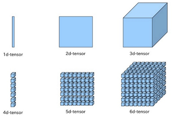
But AI needed another type of recursive processing that involved matrix math. Matrix can be done on a GPU, but it’s not the most efficient engine for it. Other approaches tried by other firms were DSPs and dedicated matrix math processors constructed in FPGAs. DSPs were (are) used successfully in mobile devices like smartphones, and Qualcomm is a leader in that area. FPGAs are functionally effective but not fast. A new, dedicated matrix math processor was needed. Google was one of the first to offer such a device, which they named a tensor processor. The mathematical definition of a tensor is an algebraic object that describes a multilinear relationship between sets of algebraic objects related to a vector space. But the straightforward way to think about it is a tensor processor does 3D processing in real time, and it is visualized as the diagram in Figure 2.
So now, the Nvidia Turing GPU being employed on the new RTX 2080 AIB (and Quadro RTX AIB) had two new ASIC-like math engines—inference engines for ray tracing, and tensor engine for matrix math. The Turing GPU was the first general-purpose consumer AI processor.
One of the other features of the new GPU was deep learning super sampling (DLSS). Nvidia claimed tensor cores could be used to improve gaming performance through DLSS. DLSS leverages a deep neural network to extract multidimensional features of the rendered scene and intelligently combine details from multiple frames to construct a high-quality final image. This allows Turing GPUs to use half the samples for rendering and use AI to fill in information to create the final image. The result, said Nvidia, is an image with similar quality as traditional rendering (which typically relies on temporal anti-aliasing in most of today’s latest games) but with higher performance. Nvidia said DLSS was an easy integration for developers, and at the time (fall 2018), developers announced 25 games would have DLSS support.
The Turing GPU was the first general-purpose consumer AI processor.
The power GPU, which already had thousands of SIMD processors, video codec processors, audio processors, display and raster operation processors, memory managers, and I/O processors, now got two new processors—RT and tensor. The Turing GPU was a tour de force.[i]
The Turing SM is partitioned into four processing blocks, each with 16 FP32 cores, 16 INT32 cores, two Tensor cores, one warp scheduler, and one dispatch unit.
The Turing architecture introduced important enhancements to the core execution data paths. Previous shader workloads consisted of a combination of floating-point (FP) arithmetic instructions, such as floating add (FADD) or floating multiply-add (FMADD), along with simpler instructions like integer adds for addressing and data retrieval, floating-point compares, or min/max for result processing, and more. In prior shader architectures, the floating-point math data path remains inactive whenever one of those non-FP math instructions was executed. Turing addressed that limitation by incorporating a second parallel execution unit alongside each CUDA core. That unit operated in parallel with the floating-point math unit, enabling simultaneous execution of both FP and non-FP math instructions.
Within the new architecture, the primary enablers for Turing’s improvement in graphics performance were a new GPU processor (streaming multiprocessor, or SM) architecture with improved shader execution efficiency, and a new memory system architecture that includes support for the latest GDDR6 memory technology.
In parallel with Turing’s development, Microsoft announced both the DirectML for AI and DirectX Raytracing (DXR) APIs in March 2018.[i]
The Turing GPU broke all records for superlative numbers with 18.6 billion transistors (fabricated on TSMC’s 12nm FinFET process), 14.2 TFLOPS of peak single-precision (FP32) performance, and two new measurements: 113.8 Tensor TFLOPS and 10 Giga rays/sec.
Turing had 4,608 shaders (CUDA cores) capable of mesh shading.[ii] [iii] Mesh shading advanced the geometry processing architecture by offering a new shader model for the vertex, tessellation, and geometry shading stages of the graphics pipeline, supporting more flexible and efficient approaches for computation of geometry.
Another new feature introduced with the Turing architecture was variable rate shading (VRS). VRS offers dynamic control over the frequency of shading in graphics rendering. Developers can adjust the shading rate, ranging from once per 16 pixels to eight times per pixel. VRS enables more efficient shading by reducing unnecessary work in areas of the screen where full-resolution shading would not visibly enhance image quality. Various categories of VRS-based algorithms have already been identified, including Content Adaptive Shading (which adjusts shading based on content level of detail), Motion Adaptive Shading (which varies shading based on the rate of content motion), and foveated rendering (which considers lens resolution and eye position, particularly in VR applications).
Texture-space shading (TSS) was yet another new development in the Turing architecture. With texture-space shading, objects are shaded in a private coordinate space (a texture space) that is saved to memory, and pixel shaders sample from that space, rather than evaluating results directly. With the ability to cache shading results in memory and reuse/resample them, developers can eliminate duplicate shading work or use different sampling approaches that improve quality.
The GPU was big, 754mm2 and 18,600 transistors—a new high in both dimensions. It also was a heavy user of power, sucking up to 280W.
But Turing was the foundation of a new generation of GPUs with dedicated ray-tracing and tensor engines, and full mesh-shading capabilities. Nvidia paid for being first and had to encourage and support game developers to embrace the new rendering approach. Most of them welcomed it, but game development takes time, and so major titles didn’t show up for a year or more. AMD held back on implementing RT acceleration, but when Intel entered the market, they offered it, and their DLSS scaling capability with the launch of their Xe GPUs in September 2020. AMD launched their first hardware RT-accelerated GPU, the Radeon RX 6000, in October 2020. By then, Nvidia was on its second generation and preparing its third.
In mid-2023, Nvidia was the undisputed leader in real-time ray tracing and shipping DLSS 3.0, which improved performance even more and allowed 4K RTRT at respectable frame rates.
You can find out more about ray-tracing technology, history, and applications in Dr. Peddie’s book Ray Tracing: A Tool for All.
[1] JPR predicts we could have real-time ray tracing on our PCs in less than six years, https://www.jonpeddie.com/news/peddie-predicts-we-could-have-real-time-ray-tracing-on-our-pcs-in-less-than/?swcfpc=1
[2] Kilgariff, E., Moreton, H., Stam N., and Bell, B. Nvidia Turing Architecture In-Depth, https://developer.nvidia.com/blog/nvidia-turing-architecture-in-depth/
[3] Announcing Microsoft DirectX Raytracing!, https://devblogs.microsoft.com/directx/announcing-microsoft-directx-raytracing/
[4] Peddie, J., Mesh Shaders and the History of Computer Graphics, https://www.computer.org/csdl/video-library/video/1CHRLWpzRUA
[5] Peddie, J., Mesh Shaders Release the Intrinsic Power of a GPU, https://blog.siggraph.org/2021/04/mesh-shaders-release-the-intrinsic-power-of-a-gpu.html/