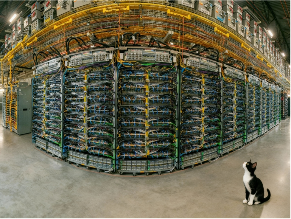
Google is expanding how it builds its AI chips. For its next-generation Ironwood TPU, debuting in 2026, it’s teaming with MediaTek and Broadcom—a move that spreads cost and production risk. MediaTek will handle I/O and manufacturing coordination with TSMC, leveraging its supply-chain strength and lower pricing. Broadcom continues developing the high-performance cores used in Google’s AI training systems. Google leads the overall design, keeping architectural control, while preparing to scale TPU production dramatically—and possibly offer some units beyond its own cloud for the first time.

Google’s Ironwood inferencing AIP pod. (Source: Google)
In March, Google announced it would partner with Taiwan-based MediaTek for its upcoming Ironwood TPU, suggesting a broader distribution strategy.
Google has partnered with MediaTek to develop the next generation of Google’s Tensor Processing Units (TPUs), internally code-named Ironwood for AI (covered here). Google hopes this partnership reduces reliance on Broadcom and improves the cost structure for high-volume AI accelerator manufacturing at scale. Production begins in 2026 at TSMC and will utilize MediaTek’s established relationships and Google’s previous TPU manufacturing processes on advanced nodes and packaging. MediaTek offers competitive pricing, supply-chain expertise, and experience that align with Google’s performance and yield goals. The collaboration advances Google’s multi-source silicon strategy, spreads risk across multiple partners, and bolsters its position in data-center AI hardware markets and services.
Google leads the core architecture design for its Ironwood TPU, the seventh-generation tensor processing unit announced at Google Cloud Next 2025 and optimized for AI inference workloads. The company relies on two specialized partners to execute different aspects of the chip development and production process ,while TSMC manufactures the processors on advanced nodes including the N3P 3 nm process.
MediaTek handles input/output module design, SerDes high-speed interfaces, and peripheral components that manage data transfer between the processor and external systems. The company coordinates production logistics with TSMC, leveraging its established relationship with the foundry to negotiate lower costs for advanced packaging technologies like CoWoS. MediaTek focuses on cost-sensitive variants such as the TPUv7e, with production scheduled to begin in 2026. Google selected MediaTek partially because the company offers costs approximately 20–30% lower than alternative partners, while maintaining strong TSMC integration capabilities. This partnership marks a strategic shift that enables Google to exert greater influence over TPU architecture decisions and expand deployment into consumer devices beyond data-center applications.
Broadcom continues its role as co-developer of the core TPU architecture, translating Google’s specifications into manufacturable silicon designs. The company provides proprietary SerDes interfaces for high-speed data transmission and oversees ASIC design processes. Broadcom manages chip fabrication coordination and advanced packaging oversight with TSMC, particularly for training-optimized variants like the TPUv7p that succeed the Trillium TPUv6e generation. The company has maintained its position as Google’s long-standing partner since the TPU program’s inception, handling designs that require high-performance capabilities for model training workloads.
TSMC fabricates the final silicon, producing chips with specifications including 700 mm² die sizes, 192 GB HBM3E memory, and 4,614 FP8 TFLOPS computational performance. Google spent over $9 billion on TPU development and deployment in 2025, driving the company’s strategy to diversify partnerships while maintaining architectural control. Meta evaluates potential TPU adoption in 2027, which would expand demand for Broadcom’s design services. The division of responsibilities allows Google to balance cost optimization through MediaTek’s manufacturing coordination with Broadcom’s design-to-fabrication expertise, creating a modular development structure that maintains Google’s oversight of critical tensor-core architecture.
Google plans to build millions of the V7 TPUs in 2026 and may consider offering some to third parties as well. If they do, that would put them in direct competition with their former partners AMD and Nvidia.
LIKE WHAT YOU’RE READING? INTRODUCE US TO YOUR FRIENDS AND COLLEAGUES.