The NextSilicon Maverick-2 features a novel Intelligent Compute Accelerator (ICA) architecture that dynamically adapts to application needs in real time, moving beyond traditional fixed GPU architectures. Its dataflow-style execution model is more flexible than classic SIMD/MIMD paradigms. The ICA’s adaptive architecture accelerates specific code segments, aiming to provide better performance per watt than traditional CPUs and GPUs. NextSilicon claims the Maverick-2 offers up to 4x better performance per watt than Nvidia’s Blackwell B200 GPU.
Elad Raz, founder and CEO of NextSilicon, introduced the company’s Maverick-2 dataflow engine. NextSilicon was founded in 2017 and has received over $300 million in funding. The company collaborated with Sandia National Laboratories on the design and testing of the Maverick-1 dataflow engine. Sandia is now building an experimental supercomputer called Spectra as part of its Vanguard-II program, which aims to evaluate and accelerate emerging technologies for future large-scale production platforms.
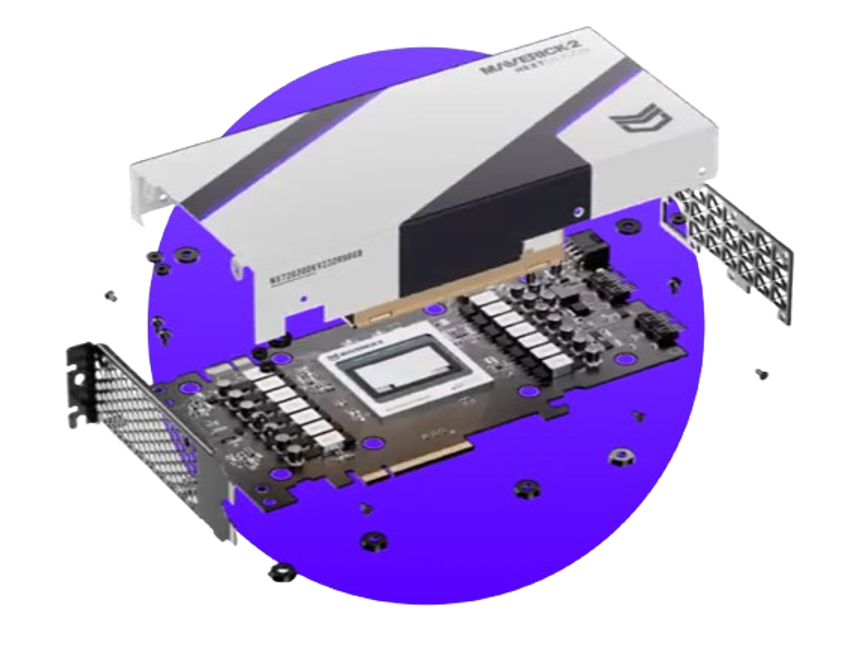
NextSilicon’s approach focuses on using software to accelerate applications. The company’s software algorithm identifies the most critical parts of the code and accelerates them. This is achieved through the dataflow engine in the compiler, which creates a graph of the data and operations in a program. The goal is to apply the Pareto principle, where 20% of the code is optimized to reduce 80% of the runtime. NextSilicon is not currently targeting the AI training and inference market.

Raz describes NextSilicon’s dataflow compiler as their key innovation. The compiler identifies compute-intensive code portions as the application runs on the host, staying in the intermediate representation of the computational graph. This approach is similar to a just-in-time compiler for hardware. The graph is placed on the dataflow hardware, and telemetry from the hardware is used to recursively optimize compute and memory as the program runs. This process involves identifying “likely flows” in the graph of the running program, allowing for continuous optimization. The goal is to optimize the program’s performance in real time.
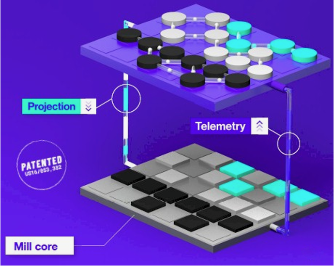
The Maverick dataflow engine projects likely and unlikely code flows onto a grid of processing and memory elements. As the code runs, performance bottlenecks are identified, and telemetry data is sent back to the Maverick compiler. The compiler then rebalances the flows, allocating more processors to likely flows and taking them from unlikely flows. This process is asymmetric, allowing for efficient optimization.
The Maverick architecture off-loads certain types of serial work to local cores or the host CPU, depending on the workload. This approach enables efficient communication between local cores and avoids cross-chip communication. The dataflow design eliminates the need for branch predictors.
A smart runtime algorithm optimizes the most frequently occurring functions, reconfiguring the chip for the most critical tasks. This approach shifts the optimization problem from static compilation to runtime, allowing the Maverick processor to execute software without requiring extensive compilation or tuning.
Through iterative rounds of telemetry and self-optimization, the Maverick processor accelerates workloads tailored to each specific application. This process results in improved developer productivity and faster time to science. Once the Maverick compiler has fully optimized the hardware configurations for likely and unlikely flows, the system creates a mill core. This optimized configuration enables efficient execution of the workload.
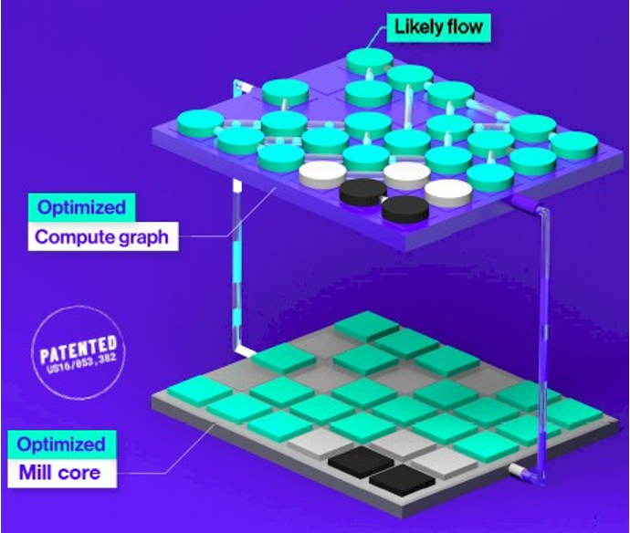
The mill cores in the Maverick dataflow engine utilize as many resources as possible and off-load application snippets to optimize performance. These software-defined cores are created dynamically to run frequently used code portions. Unlike traditional SIMD units, mill cores execute independent tasks coordinated by a runtime scheduler, rather than executing the same instruction in lockstep.
The mill cores are optimized for throughput and power efficiency, rather than latency and brute-force. They can run hundreds or thousands of data streams in parallel and be replicated across the dataflow engine for parallel processing. This architecture allows for massively parallel processing, accelerating runtimes significantly.
The Maverick-2’s architecture doesn’t fit neatly into traditional SIMD or MIMD categories; instead, it uses a dataflow-style execution model that’s more flexible than traditional paradigms. By replicating hundreds of mill cores and running thousands of data streams, the Maverick-2 achieves parallel processing capabilities similar to those of conventional CPUs or GPUs. This approach enables the Maverick-2 to accelerate runtimes by leveraging its unique architecture.
Accelerate what matters
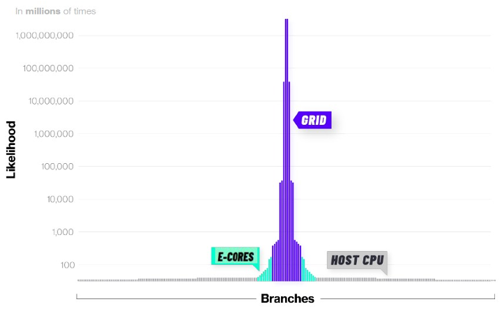
Another key process involves loading the workload algorithm and data onto the Maverick dataflow engine and keeping as much of it there as possible to minimize data movement. By achieving this, the workload is divided into likely flows, reasonably likely flows, and unlikely flows, which follows a distribution similar to a Gaussian distribution. This distribution is crucial for optimizing the performance of the Maverick dataflow engine, which resembles a Gaussian distribution like the one shown in Figure 4.
NextSilicon created a radar graph that shows the characteristics of the Maverick dataflow engine compared to CPUs, GPUs, and FPGAs.
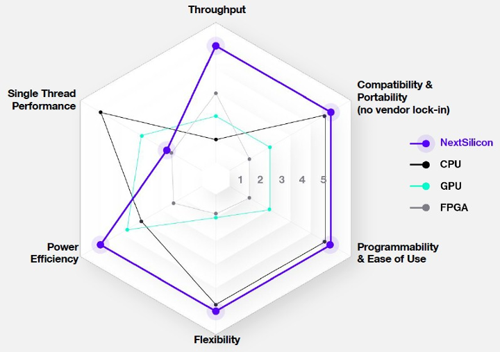
The goal was to get the programmability, flexibility, and portability of a CPU and better power efficiency and throughput than a GPU or FPGA while sacrificing on single-threaded performance, which can be off-loaded to Maverick E-cores or the host CPU.
NextSilicon has not revealed which processor was used for the E-cores on the Maverick-2 chip, but they are most likely Arm or RISC-V.
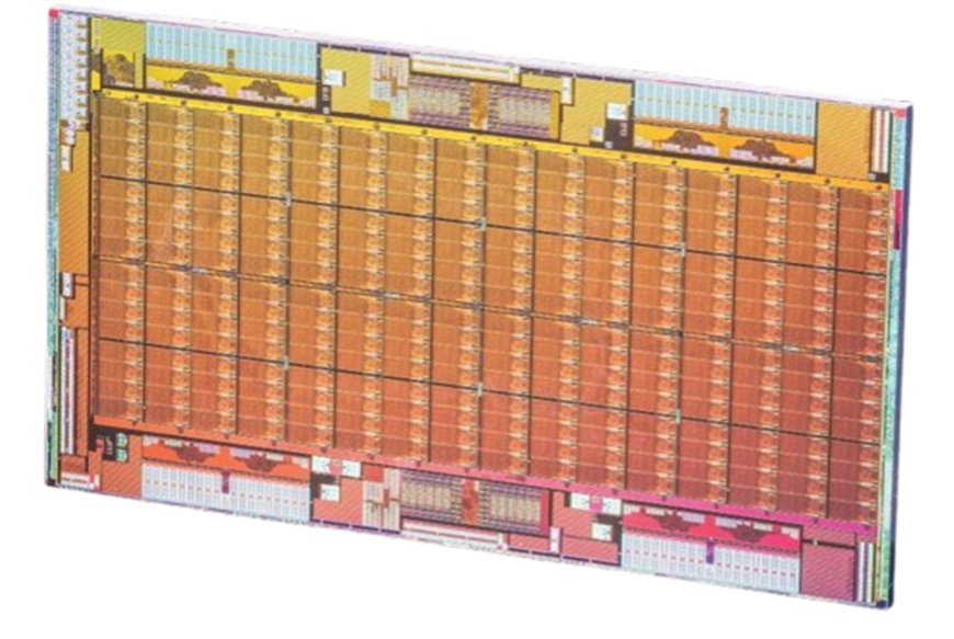
The die shot suggests there are two four banks of 24 E-cores and what looks like 256 compute elements.
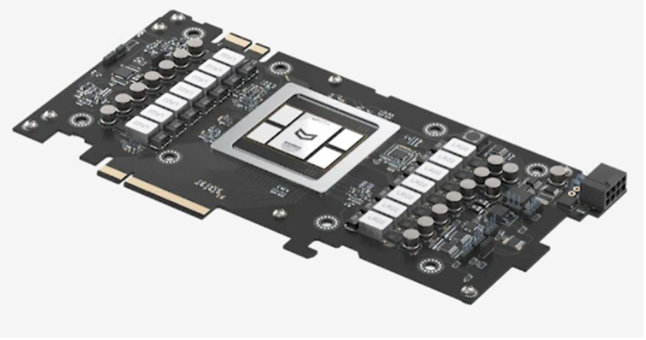
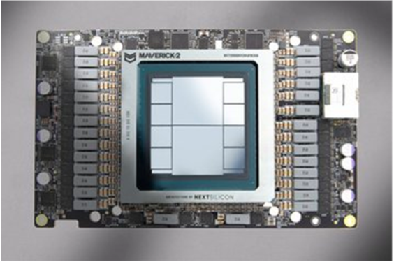
The company has also developed a second version of the processor, shown in Figure 8.
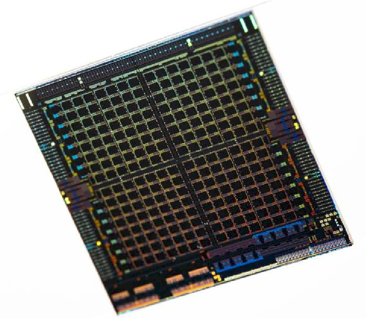
The Maverick-2 architecture features 32 embedded cores and 224 compute elements, organized into four blocks of 7x8 grids of compute units. This design enables the accelerator to efficiently handle high-performance computing (HPC) and AI workloads. The chip is fabricated using TSMC’s 5 nm process and has an area of 615 mm². It operates at a clock speed of 1.5 GHz, with both the embedded cores and dataflow processing elements running at the same speed.
The company may explore overclocking the embedded cores to accelerate serial work in the future. In the data center, the Open Accelerator Infrastructure (OAI) organization, a subgroup of the Open Compute Project (OCP), has been defining AI accelerator card form factors known as OCP Accelerator Modules (OAMs) since 2019. These OAMs typically form a POD and are incorporated into a single-rack chassis, providing a standardized approach to AI acceleration in data centers and supercomputers. This standardization effort aims to improve the efficiency and scalability of AI infrastructure.
The OAM form factor introduced by Microsoft and Meta was to get a universal accelerator socket for data center accelerators. Intel and AMD use the OAM socket for their accelerators; Nvidia does not. The OAM version only exposes a total of 16 lanes of PCI Express 5.0 I/O to the outside world, instead of 32 lanes.
The Maverick-2 has four banks of HBM3E memory.
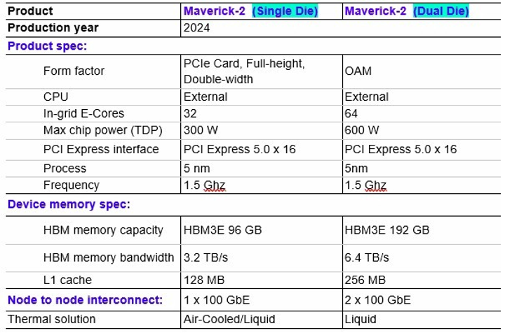
NextSilicon claims that the Maverick-2 will outperform Nvidia’s Blackwell B200 GPU by a factor of 4 in terms of performance per watt. The B200 has a power consumption ranging from 1,000W to 1,200W, whereas a single Maverick-2 chip consumes 300W, and a pair in an OAM package consumes 600W. Each Maverick chip has a thermal design point of 300W, and the OAM unit, which is only available in a liquid-cooled version, is rated at 600W.
In high-performance computing (HPC) simulations, NextSilicon asserts that the Maverick-2 delivers over 20 times the performance per watt of a 32-core Intel Sapphire Rapids Xeon Platinum SP-8352Y processor. This processor is rated at 1.8 TFLOPS at FP64 precision on its AVX-512 vector units and consumes 205W.
However, NextSilicon notes that the strength of the Maverick compiler and its ability to create and replicate mill cores in the dataflow engine are being tested as much as the FP64 and FP32 performance of the chip. This suggests that the Maverick-2’s performance advantages may be due in part to its innovative compiler and dataflow architecture.
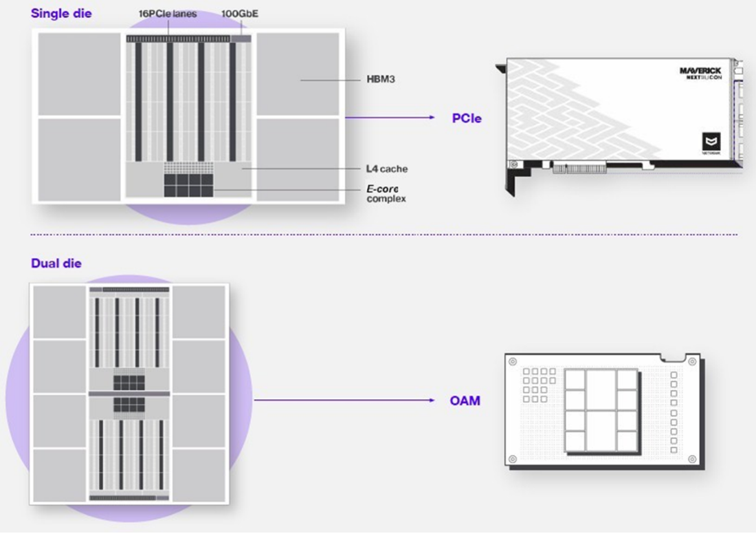
The Maverick-2 chip features a 100 Gbps Ethernet port, enabling the connection of multiple accelerators. However, NextSilicon has not disclosed the maximum number of Maverick-2 devices that can be linked together in a shared memory cluster.
Maverick-2 chips are compatible with C, C++, and Fortran applications, and can be used with OpenMP and Kokkos frameworks. NextSilicon plans to expand this support in the future, with plans to run AMD’s HIP/ROCm, Nvidia’s CUDA, and other AI frameworks on the Maverick-2 chips.

In addition, the company was selected to participate in ODISSEE (Online Data Intensive Solutions for Science in the Exabytes Era), a major European Union project to process and analyze unprecedented volumes of scientific data.
Epilog
Dataflow processors have their roots in the 1960s, when Jack Dennis and his graduate students at MIT pioneered the concept of dataflow programming. This approach models programs as a directed graph of data flowing between operations, enabling parallel processing and efficient data handling. Dennis and his team introduced the first dataflow compiler in the 1970s.
While dataflow processors haven’t yet achieved widespread commercial success, they’ve influenced specialized hardware and software architectures, particularly in areas like digital signal processing, network routing, and artificial intelligence.
In December 1985, NEC introduced its dataflow chip, the μPD7281 Image Pipelined Processor (IMPP). This single-chip dataflow system was designed for signal processing applications, particularly for fast and small algorithms. The IMPP was used in various projects, including the development of a Wavefront Array Processor with reconfigurable interconnections and processor addressing schemes for large arrays.
The μPD7281 IMPP was part of NEC’s efforts to develop advanced dataflow processing technologies.
Another notable example of a commercially successful dataflow computer is the Intel i860 processor, released in 1989. The i860 was a 64-bit microprocessor that incorporated dataflow architecture and was designed for high-performance computing applications, including graphics, simulation, and scientific computing. The Intel i860 was a significant milestone in the development of dataflow computing, demonstrating the potential of dataflow architecture in commercial applications.
Dataflow machines have faced several challenges that have limited their widespread adoption. One major issue is the complexity of their design, which requires intricate management of data dependencies, scheduling, and synchronization. This complexity has historically made dataflow machines more expensive to develop and manufacture.
In terms of performance and efficiency, dataflow machines often incur overhead due to the need to manage data dependencies and synchronization. Additionally, they can struggle to efficiently utilize resources such as processing units and memory.
Furthermore, dataflow machines require specialized programming models and languages, which can be difficult to learn and use. The lack of widely adopted software frameworks and tools for dataflow machines has also limited their appeal to developers. These challenges have hindered the adoption of dataflow machines, despite their potential benefits.
Nevertheless, researchers continue to explore dataflow machines and their applications, particularly in areas like artificial intelligence, machine learning, and high-performance computing.
LIKE WHAT YOU’RE READING? INTRODUCE US TO YOUR FRIENDS AND COLLEAGUES.