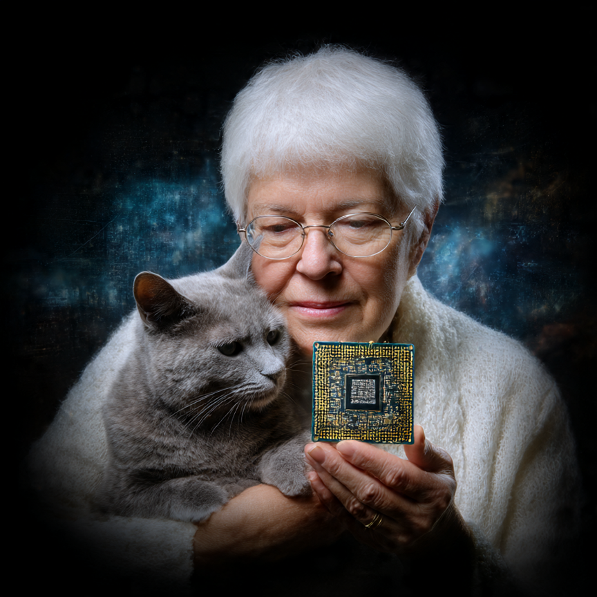
Nvidia is quietly preparing its next big leap—the Vera Rubin chip, a fusion of an Arm-based Vera CPU and a Rubin GPU built for massive AI workloads. Together they promise lightning-fast training and inference with up to 8 EFLOPSs of performance and 288GB of HBM4 memory. Already in fabrication at TSMC, Vera Rubin aims to power the next wave of generative AI, from video creation to autonomous agents, by late 2026.

Nvidia has begun signaling details of its next-generation AI processor, Vera Rubin, a combined CPU–GPU platform similar in concept to AMD’s APU designs. The platform integrates a new Arm-based Vera CPU with the Rubin GPU, the direct successor to the current Blackwell architecture, targeting the heavy computational demands of AI training and inference.
The design centers on two core chips: the Rubin GPU and Vera CPU. Each GPU employs two reticle-sized dies and delivers up to 50 PFLOPs of FP4 compute, supported by 288GB of HBM4 memory. The Vera CPU integrates 88 custom Arm cores optimized for tightly coupled AI workloads. The top configuration, Vera Rubin NVL144 CPX, combines multiple modules to reach approximately 8 EFLOPS of total AI throughput and 100TB of unified high-speed memory. Performance projections indicate about 3.6 EFLOPS in FP4 inference and 1.2 EFLOPS in FP8 training, a roughly 3.3× performance gain over the GB300 NVL72 system.
Rubin introduces higher compute density, wider memory bandwidth, and faster interconnects. Each GPU module provides 50–100 PFLOPs FP4 performance and links through NVLink 144 and Spectrum-X networking. The system’s design accommodates emerging workloads such as million-token language models, generative video synthesis, and autonomous multi-agent operations, emphasizing responsiveness and low-latency communication between compute units.
The platform has completed tape-out and entered fabrication at TSMC, with mass availability planned for late 2026. Nvidia states that Rubin and Vera will use TSMC’s 3 nm process family with HBM4 integration. Neither company has identified the exact production site. While TSMC Arizona recently began fabricating Blackwell (4 nm) wafers for Nvidia, Rubin’s manufacturing requirements depend on 3 nm process technology and advanced HBM4 packaging currently concentrated in Taiwan. Based on existing roadmaps, the first Rubin wafers are expected to originate from TSMC’s Taiwan facilities. US production could follow once Arizona’s 3 nm and HBM4 flows reach maturity, but no timeline has been confirmed.
The Vera Rubin architecture marks Nvidia’s shift toward integrated AI compute—bringing CPU, GPU, and high-bandwidth memory closer together to improve efficiency, scalability, and interoperability for the next generation of edge-to-data center AI workloads.
Vera Florence Cooper Rubin (1928–2016) was an American astronomer who pioneered work on galaxy rotation rates. She uncovered the discrepancy between the predicted and observed angular motion of galaxies by studying galactic rotation curves.
LIKE WHAT YOU’RE READING? INTRODUCE US TO YOUR FRIENDS AND COLLEAGUES.