
Qualcomm just detailed how its High Bandwidth Compute (HBC) architecture tackles a costly hidden problem in AI: moving data. HBC stacks DRAM directly onto a logic die and performs data-hungry operations where the data lives, cutting the need for wider interfaces between memory and processor. Dragonfly AI250 will ship with HBC Gen 1, and Dragonfly AI300 will carry Gen 2. For ISVs tuning inference stacks and silicon teams weighing packaging options, this shift changes how the industry measures AI performance.
Generative AI workloads expose a limit that raw compute speed cannot fix. Generating each token requires reading enormous quantities of model parameters and accumulated context from memory, and the arithmetic itself costs little compared with the job of feeding it. Compute capability climbed steeply over the past decade; memory bandwidth climbed far more slowly. Transformer model sizes grew roughly 240× every two years, and AI hardware memory grew only 2× in that same span. That divergence leaves a growing share of every accelerator idle, waiting for operands to arrive.
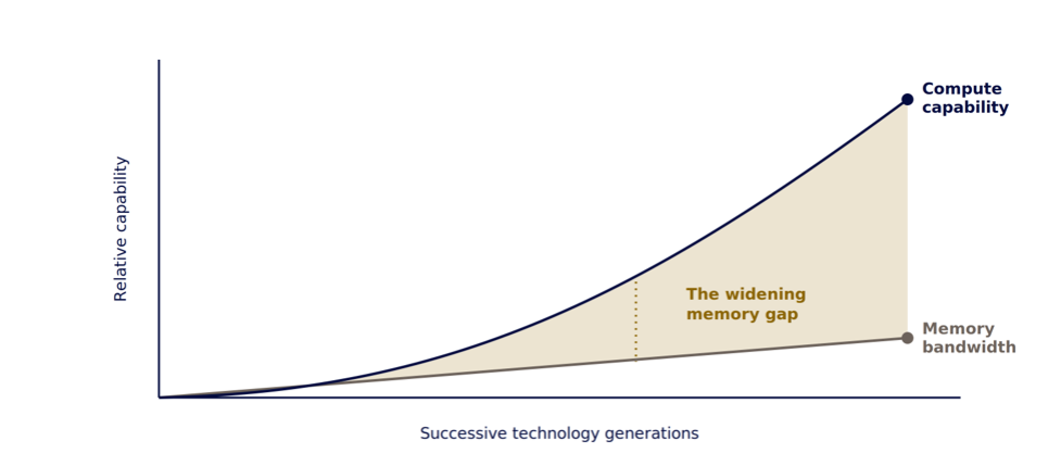
Figure 1. Compute capability climbed steeply for generations. Memory bandwidth grew far more slowly, and that gap increasingly sets real-world AI performance. (Source: Qualcomm)
The industry’s usual fix pushes more bandwidth through the same basic layout: keep memory and compute as separate components and widen the pipe between them. That approach hits physical and economic limits. Wider interfaces demand more wires and pins, adding cost and complexity with each step and shrinking the payoff each time. Every bit that travels between separate memory and compute dies burns energy and time, and at today’s scale, that movement dominates the power budget. Advanced memory-integration techniques, including 2.5D interposers such as CoWoS, carry high costs and face supply constraints, putting top-tier performance out of reach for many deployments.
Qualcomm’s answer: Move logic next to memory
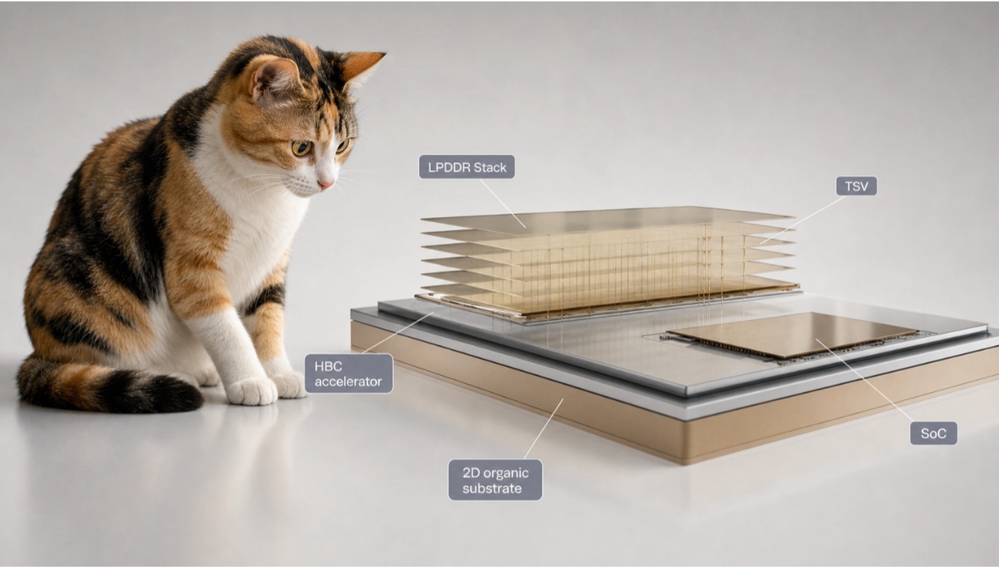
Qualcomm’s HBC architecture places compute logic directly beside memory, cutting out the chip-boundary crossing that data must otherwise make to reach it. The design stacks an LPDDR DRAM package vertically on top of a logic or compute die, connecting the layers through dense through-silicon vias (TSVs) in place of a traditional long-edge HBM interface. HBC sits on a standard 2D organic substrate, which lets Qualcomm skip supply-constrained 2.5D interposer packaging entirely. Qualcomm frames this design as near-memory computing, distinct from compute-in-memory approaches, and reports up to 6× higher bandwidth per watt than traditional HBM, along with far higher capacity per watt than on-chip SRAM delivers.
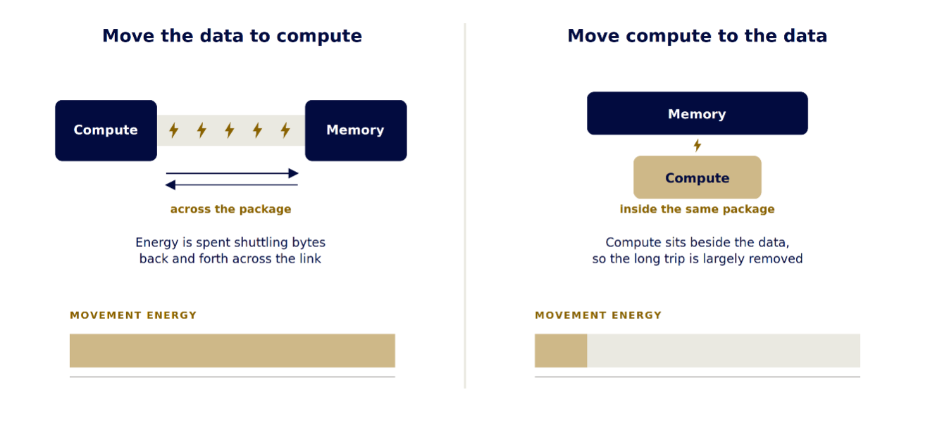
Figure 2. Two philosophies: Once data movement dominates the energy budget, computing beside the data instead of shipping reshapes system economics. (Source: Qualcomm)
The architecture does not replace the main processor. A Qualcomm Dragonfly AI accelerator continues to handle complex, flexible orchestration work, and HBC takes on the memory-bound operations that are expensive to feed. Each component performs the job its design fits.
Roadmap and rollout
Qualcomm built HBC Gen 1 into the Dragonfly AI250 rack-scale platform, which will deliver 133 TB/s of effective bandwidth per card and represents an 18× increase in effective memory bandwidth over the Dragonfly AI200’s LPDDR5X setup. HBC Gen 2 arrives with the upcoming Dragonfly AI300 platform and targets a 54× increase over the AI200 baseline. Qualcomm’s Durga Malladi, EVP and GM, Technology Planning, Edge Solutions & Data Center,speaking at a recent analyst meeting, reiterated the roadmap the company introduced at its Investor Day and confirmed first-generation HBC commercialization for fiscal 2027, with the current focus on moving from research and test chips to shipping products.
Qualcomm also positioned HBC as a modular infrastructure component, separate from any single Qualcomm platform. We would expect customers to adopt Qualcomm CPUs alone, HBC alone, or both together, independent of Qualcomm’s other accelerator offerings. That framing extends to Qualcomm’s inference strategy overall: The company expects AI deployment to spread across cloud, edge, and hybrid environments, and it plans to support models drawn from the broader ecosystem, skipping the build-out of proprietary foundation models. Qualcomm described efficiency, measured in energy consumption and token-generation throughput, as an increasingly critical competitive metric.
The Modular software stack, acquired recently, adds another piece to the pitch. It runs on third-party hardware platforms, and Qualcomm presents it as open and broadly accessible, claiming meaningful performance gains over existing stacks. Qualcomm reported strongly positive feedback from hyperscalers during early engagements.
Analysts focused their questions on implementation: Packaging technology, TSV alignment, thermal limits, memory-vendor participation, optical interconnects, yield, software-ecosystem impact, JEDEC standards alignment, and future disaggregated memory architectures all came up in Q&A. Qualcomm kept many specifics confidential, citing ongoing collaboration with memory partners and unannounced product plans.
Redefining the scorecard
Qualcomm argues that AI infrastructure buyers need a new scorecard. Headline compute figures carry less weight as buyers evaluate platforms on delivered performance for memory-bound workloads and on performance per watt and per dollar, moving focus away from peak theoretical throughput. Energy stands out as both the dominant operating cost and the binding physical constraint at hyperscale, giving architectures that minimize data movement a structural advantage that grows with scale. Memory itself takes on a more active role in this picture, shifting from a passive store to a participant in computation, with implications reaching from chip design to data center economics.
Qualcomm’s pitch treats HBC as a direct answer to a structural problem: Computing’s scarce resource shifted from raw arithmetic to the timely, affordable delivery of data. The company’s roadmap, from Gen 1 on the AI250 through Gen 2 on the AI300, gives ISVs and silicon teams a concrete target to design against, and it gives CIOs and IT buyers a new lens for comparing AI infrastructure investments beyond peak FLOPS claims.
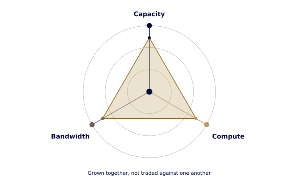
Figure 3. Capacity, bandwidth, and compute grow together with HBC. Conventional designs force trade-offs among them. (Source: Qualcomm)
For silicon teams, the near-memory approach reopens packaging choices that CoWoS supply limits closed off, and for ISVs, it puts a premium on software that schedules work around memory locality, not just raw core counts. CIOs evaluating multi-year AI infrastructure contracts gain a second lens beyond peak FLOPS: total energy per token served, a metric that scales directly with operating budgets as fleets grow.
What do we think?
HBC gives Qualcomm a credible entry into inference infrastructure without chasing Nvidia and AMD on raw compute. The near-memory approach addresses a real physical constraint, and standard-substrate packaging sidesteps CoWoS supply limits that squeeze competitors. Commercialization sits two fiscal years out, so execution risk remains, and memory-vendor cooperation will shape how fast Gen 2 reaches scale.
Inflection point. HBC marks a possible inflection point in AI infrastructure design. The industry built a decade of accelerators around adding compute and widening memory interfaces, and Qualcomm’s data suggests that path runs out of headroom as workloads scale. If near-memory architectures spread across data center, PC, automotive, XR, and industrial designs, the inflection point moves the competitive battleground from peak FLOPS to bandwidth per watt, reshaping how ISVs optimize software and how CIOs score AI infrastructure purchases across a multi-year buying cycle.
AND IF YOU LIKED WHAT YOU READ HERE, DON’T BE STINGY, SHARE IT WITH YOUR FRIENDS.