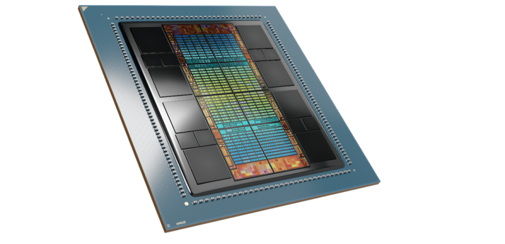
During AMD’s recent announcement, the upcoming CDNA GPU-based Instinct MI300X AIB showcased an astonishing 192GB of HBM3 memory integrated into chiplets on the GPU substrate. The high-performance gaming Radeon RX 7900 XTX AIB, launched last November, featured the Navi 31 XTX and DirectX 12 Ultimate compatibility for advanced gaming features. The Navi 31 chip boasts 6,144 SIMD cores, 384 texture mapping units, 192 ROPs, and 96 ray-tracing acceleration cores. Equipped with 24GB of GDDR6 memory, it’s nothing like the MI300 compute-oriented GPU that AMD introduced at CES in January.
At AMD’s announcement of its new powerhouse Epyc processor and a reveal of its forthcoming Instinct MI300X AIB, one of the features of the new CDNA GPU-based AIB was a mind-blowing 192GB of HBM3 scattered around the substrate of chiplets making up the GPU.
The CDNA GPU is the computer equivalent of the gaming RDNA GPU, doubled up—well, not really equivalent.
AMD launched the high-performance gaming AIB Radeon RX 7900 XTX on November 3, 2022. Built using TSMC’s 5nm manufacturing process and powered by the Navi 31 graphics processor, specifically the Navi 31 XTX variant, the AIB is compatible with DirectX 12 Ultimate. That ensures compatibility with all modern games and guarantees features like hardware ray tracing and variable-rate shading in upcoming titles.
The Navi 31 chip is large, measuring 529mm² and contains an impressive 57,700 million transistors. It has 6,144 SIMD cores (shading units), 384 texture-mapping units, 192 ROPs, and 96 ray-tracing acceleration cores.
The Radeon RX 7900 XTX is equipped with 24GB of GDDR6 memory connected via a 384-bit interface. The GPU operates at a base frequency of 1,855MHz, with a boost clock of up to 2,499MHz, while the memory runs at 2,500MHz (20Gb/s effective).
The predecessor MI300, also built on TSMC’s 5nm process, has a die size of 1,017mm² and a transistor count of 146,000 million—it’s a very big chip. However, the MI300 does not support DirectX. For GPU compute applications, OpenCL version 3.0 can be used. It features 3,520×4 SIMD core, 220×4 texture-mapping units, and 0 ROPs.

A huge memory array for AI training and even instancing makes sense. But modern games aren’t written to take advantage of such a big memory. Using scheme like resizable bar and NVMe SSD have made games run as fast as needed, which is illustrated by smoother and fewer video cuts to load new maps. Also, HBM isn’t cheap, and gaming AIBs are already reaching the point where only wealthy people can afford them.
HBM is the dividing line, or technology between consume and compute GPUs. And though they may share certain features like manufacturing process, the PCIe interface, and a sea of SIMD cores, they don’t share APIs or ROPs, and eventually will lose TMU and RT.