
AMD just showed its full answer to Nvidia’s Rubin, and it’s not a single chip, it’s an entire rack. The Instinct MI455X packs 320 billion transistors, 432 GB of HBM4 memory, and a completely new CDNA 5 architecture built to scale to 72 GPUs in one shared-memory pod. We walk through what changed under the hood, how AMD’s own Helios rack ties it together, and how the specs stack up against Nvidia’s competing platform, chip for chip and rack for rack.
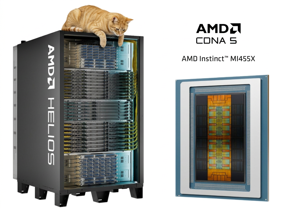
(Source: AMD)
AMD introduced the Instinct MI455X at its Advancing AI 2026 event, positioning the chip as its direct answer to Nvidia’s Rubin. The GPU replaces the MI355X atop AMD’s data center lineup and runs on a new CDNA 5 architecture built from the ground up for rack-scale AI deployment. CDNA 5 marks a real architectural break: The GCN microarchitecture powered every AMD compute accelerator for close to 15 years, from Tahiti through Fiji, Vega, and four generations of CDNA. CDNA 5 moves to a design based on AMD’s RDNA graphics lineage instead, closing out GCN’s run and opening a new one.
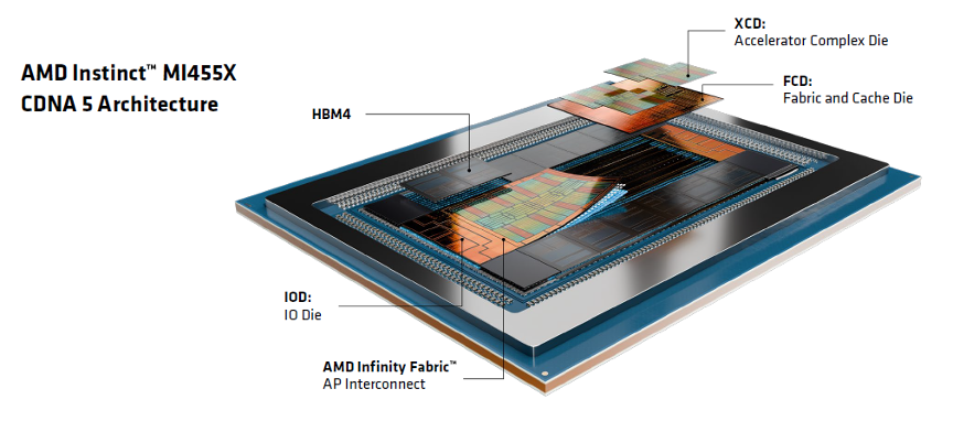
Figure 1. The CDNA 5 architecture with the different dies. (Source: AMD)
The chip carries 320 billion transistors across a chiplet package built with TSMC’s CoWoS-L advanced packaging and 3D hybrid bonding. Eight Accelerator Complex Die chiplets, or XCDs, handle compute; AMD fabricates those on TSMC’s N2 process. Two Fabric and Cache Dies, or FCDs, handle memory and cache duties, fabricated on TSMC’s N3P process. The hybrid bonding delivers denser die-to-die connections than earlier packaging generations, lifting compute density and performance per watt. Nvidia’s Rubin carries 336 billion transistors, a modest 16 billion-transistor edge that doesn’t translate into a clean compute advantage once the full spec sheet comes into view.

Figure 2. Overall conceptual view of the AMD Instinct MI455X GPU. (Source: AMD)
Inside each XCD, AMD replaced the 32 compute units of the prior generation with 32 Work Group Processors, splitting each XCD into two shader engines of 16 WGPs apiece. That gives the full chip 256 active WGPs (272 physical, with eight disabled for yield), running at up to 2.4 GHz. Each WGP swaps the old Wave64 execution model for Wave32, cutting instruction latency, branch divergence penalties, and register pressure, and making it easier for software to map tensor tiles onto hardware. Every WGP now packs four 32-thread SIMD units alongside four scalar units, capable of 256 packed FP32 operations per cycle. The matrix units scale further still: each handles up to 8,192 FP4 operations per cycle, and four matrix units per WGP push that to 65,536 matrix operations per cycle at the WGP level.

Figure 3. Relationship of compute and memory resources in the AMD Instinct MI455X GPU—does the “M” stand for massive? (Source: AMD)
The net result: 40 PFLOPS of FP4 compute and 20 PFLOPS of FP8, double the MI350 series, with peak FLOPS on the OCP microscaling MXFP4 and MXFP8 formats running 4× higher than MI355X. Rubin, by comparison, claims 50 PFLOPS of FP4 and 17.5 PFLOPS of FP8. The register file grew to match: A single wave can now address up to 1,024 vector registers, four times the 256 available on MI355X, letting 64 resident waves occupy a single WGP. Cache capacity doubled too, with 64 KB of L1 data cache and 320 KB of local data store per WGP, adding up to 192 MB of L2 across the whole chip, split across the two FCDs and delivering 54 TB/s of aggregate L2 bandwidth.
Memory saw the biggest single jump in the platform. Twelve stacks of HBM4, each running a 2,048-bit interface, double the bit width of the prior HBM3E generation, give the MI455X 432 GB of capacity, a 50% increase over MI355X’s 288 GB, and 23.3 TB/s of bandwidth, nearly triple the previous chip’s 8 TB/s. Rubin ships 288 GB of HBM4 at 22 TB/s, putting AMD ahead on capacity by roughly 1.5× and running essentially even on bandwidth. New multicast load instructions let one memory read feed multiple WGPs at once through a Broadcast Arbitrator at each shader engine, cutting redundant traffic for workloads like matrix multiplication where many compute units need the same operand. AMD also added a Tensor Data Mover unit to every WGP, purpose-built to handle tensor tiling across up to five dimensions and to move data directly between local storage and DRAM without staging it through registers first.
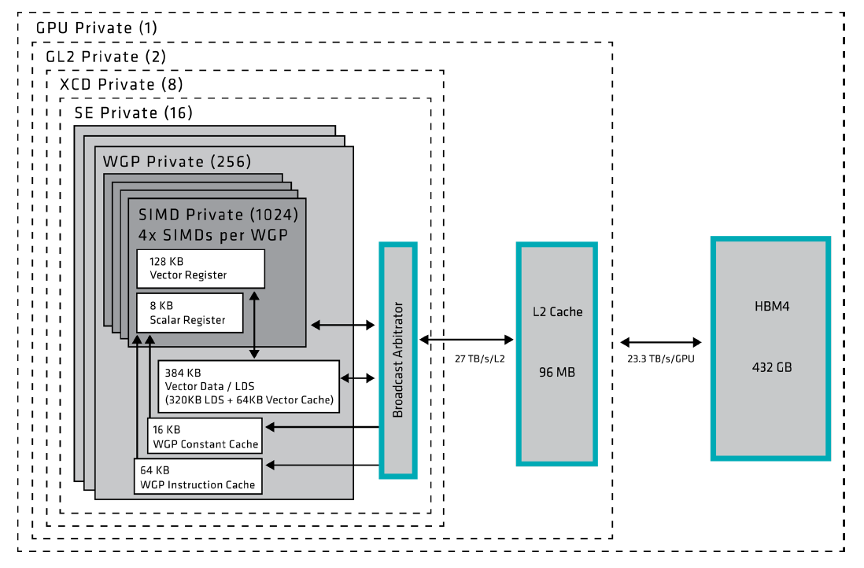
Figure 4. AMD Instinct MI455X GPU memory subsystem hierarchy. (Source: AMD)
Scaling beyond a single chip is where AMD made its largest architectural investment. The MI355X shipped with seven Infinity Fabric links delivering 1.07 TB/s of total scale-up bandwidth. MI455X jumps to 36 UALoE links, each carrying 400 Gb/s over two 200 Gigabit Ethernet lanes, for 3.6 TB/s of peak bidirectional bandwidth per GPU. A new split DMA architecture automatically routes traffic across the optimal link and hides the interconnect topology from software entirely, so communication libraries don’t need topology awareness built in. Scale-out bandwidth climbed just as sharply, up to 600 GB/s per GPU through as many as three AMD Pensando Vulcano 800 AI NICs, six times MI355X’s scale-out capacity. AMD’s Helios rack ties 72 MI455X GPUs into one shared-memory pod across 18 compute trays, each carrying four GPUs and a 96-core Epyc 9006 SP7 host CPU with a terabyte of DDR memory. Six switch trays deliver 260 TB/s of aggregate bidirectional scale-up bandwidth, and scale-out networking adds up to 43 TB/s more. A full rack totals 2.9 EFLOPS of FP4 compute, 31 TB of shared HBM4, and 1.7 PB/s of aggregate memory bandwidth.
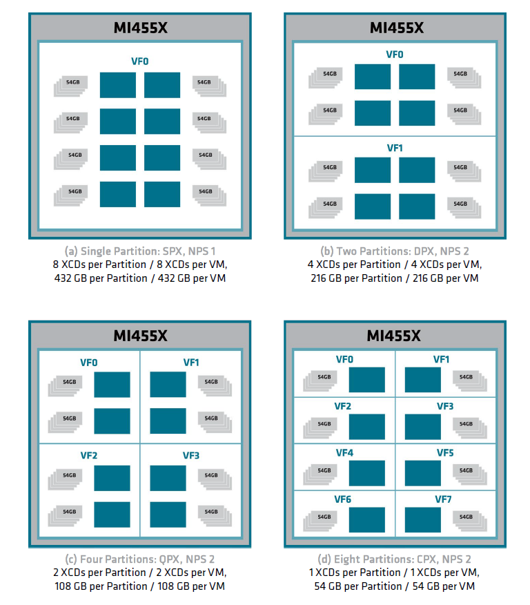
Figure 5. Spatial partitioning configurations for the AMD Instinct MI455X GPU. (Source: AMD)
A dedicated Infinity Fabric link, separate from the scale-up and scale-out interconnects, replaces PCIe for CPU-to-GPU communication, running 256 GB/s bidirectionally and giving the host CPU cache-coherent access to GPU memory. Security features include a silicon root of trust, support for the DMTF’s SPDM specification, a trusted execution environment with trusted I/O, and single-root I/O virtualization, letting operators isolate up to eight partitions per GPU for multi-tenant deployments. AMD claims the payoff shows up directly in inference economics: up to 34× higher token throughput and 18× lower cost per token versus MI355X. Against Rubin, AMD’s own comparison claims 1.5× the memory capacity, 1.5× the scale-out bandwidth, and roughly matching figures on memory bandwidth, FP4/FP8 compute, and scale-up bandwidth. A third chip, the MI430X, aims at sovereign AI and HPC workloads specifically, pairing the same 432 GB HBM4 memory pool with 288 TFLOPS of hardware FP64 performance and hybrid CPU+GPU compute, shipping in the first half of 2027.
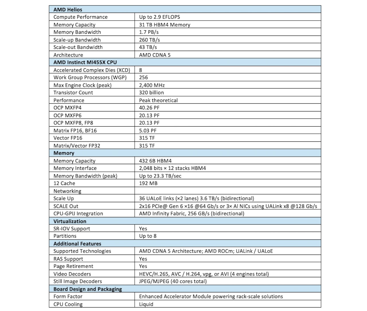
Table 1. AMD Helios and Instinct MI455X GPU feature summary. (Source: AMD)
None of these numbers exist in isolation from AMD’s broader stack. The MI455X shares its socket, its networking silicon, and its software stack with the rest of AMD’s data center lineup, and every capability above reaches developers through ROCm without hardware-specific tuning. That’s the real bet behind CDNA 5 architecture: a full rack, from Epyc CPUs to Pensando NICs to Helios switches, built to scale as one unit and sold as one open platform, beats a single chip competing alone.
What do we think?
MI455X closes AMD’s spec gap with Rubin and wins on memory capacity, the metric that gates large-model deployment today. The CDNA-to-RDNA architectural switch matters more than any single benchmark: AMD retired 15 years of GCN lineage in one generation. For CIOs, the real decision point isn’t the chip, it’s ROCm maturity and whether Helios racks ship on schedule in volume.
Inflection point
CDNA 5 is an inflection point for AMD, not a spec bump. Abandoning 15 years of GCN lineage for an RDNA-based architecture, mid-fight with Nvidia over the AI accelerator market, signals AMD believes the old design had hit its ceiling. Pair that with Helios scaling to 72 GPUs as one shared-memory pod, and AMD is no longer selling chips, it’s selling rack-scale systems. Whether ROCm matures fast enough to make that pitch land determines if this becomes AMD’s Nvidia-rival moment.

LIKE WHAT YOU’RE READING? TELL YOUR FRIENDS; WE DO THIS EVERY DAY, ALL DAY.