
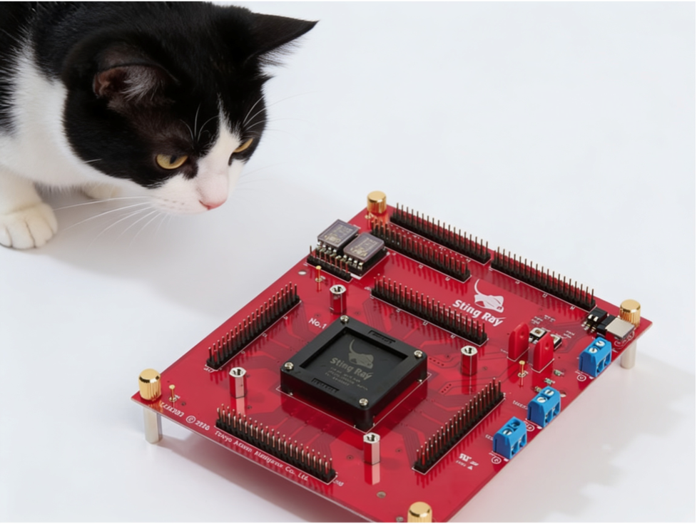
Tokyo Artisan Intelligence wants AI to work where infrastructure actually lives: railways, factories, public systems, robots, cameras, and sensors. The Yokohama start-up has moved from edge AI systems into reconfigurable AI semiconductor development with partners Oppstar, Silicon X, and UMC. Its Seaside-R6 platform already targets harsh field environments. Its Sting Ray test chip points toward a custom edge AI path focused on low power, low latency, heat control, and site
(Source: TAI and JPR)
Tokyo Artisan Intelligence, or TAI, has chosen a precise AI silicon problem. The company targets edge systems that must make decisions locally, without sending every camera frame or sensor event to the cloud. That focus leads TAI toward railways, manufacturing, infrastructure, robotics, and public safety, where latency, heat, power, vibration, bandwidth, and maintenance access matter as much as model accuracy.
TAI started in 2020 as a Tohoku University-linked company building edge AI systems for worksite inspection. CEO Hiroki Nakahara, a professor at Tohoku University, moved the company toward custom silicon after field deployments exposed limits in off-the-shelf processors. Edge devices often live inside cramped housings, near tracks, above platforms, beside roads, inside factories, or on mobile inspection carts. In those settings, heat can turn a compute choice into a reliability problem.
The company’s current platform, Seaside-R6, gives it a practical base. TAI describes Seaside-R6 as an edge AI computing platform designed for harsh industrial, railway, and construction-site environments. It supports current AI models, multiple cameras and sensors, rich I/O, durability testing, and mass-production sourcing. That platform gives TAI a system-level starting point before its custom reconfigurable AI chip reaches production.
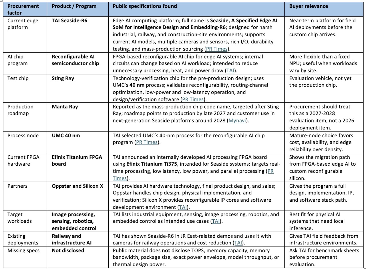
Table 1. Tokyo Artisan Intelligence Co. Ltd.’s Seaside specifications.
TAI’s silicon story does not fit the usual NPU label cleanly. The company describes a reconfigurable AI semiconductor chip based on FPGA ideas. That means the device can alter internal circuit behavior according to an application or model, rather than forcing every workload through a fixed accelerator shape. For silicon teams, that distinction matters. TAI aims to keep FPGA-like flexibility and remove wasted logic, power, and heat from specific edge inference deployments.
The first custom silicon step uses Sting Ray, a test chip for technology verification. TAI says Sting Ray validates reconfigurability, routing-channel choices, low-power behavior, low-latency operation, and design and verification software. The company selected UMC’s 40 nm process, a mature node that fits the cost, availability, and reliability priorities of industrial AI hardware. Edge AI does not always need an advanced node. It needs enough performance inside a thermal envelope the site can support.
TAI has also mapped a production path. Reports identify Manta Ray as the mass-production chip code name, following Sting Ray. The roadmap points to production by late 2027 and customer use in next-generation Seaside platforms around 2028. CIOs should treat that timing as an evaluation runway. The current Seaside-R6 platform can support near-term field work, and the custom chip belongs in procurement planning for future refreshes.
The Oppstar partnership gives TAI access to semiconductor design execution beyond its own AI systems work. Oppstar handles chip design, physical implementation, and verification. Silicon X supplies reconfigurable IP cores and software development environment work. TAI provides AI hardware technology, final product design, and sales. That division of labor gives the program a practical path from field requirements to silicon, package, software, and customer system.
The collaboration also matters for Malaysia. Oppstar’s role moves the country’s semiconductor story beyond assembly and test into front-end IC design. TAI also gains access to a regional design ecosystem, Arm-based IP economics, and engineering capacity. Japan wants to rebuild parts of its semiconductor base. Malaysia wants more value from chip design. TAI’s project sits at that intersection.
The use cases make the hardware case clearer. Railway operators need track inspection, station safety monitoring, disaster monitoring, and equipment checks. Factories need visual inspection, anomaly detection, and robotics support. Public road and power-line infrastructure need field sensing and local alerts. These applications often need decisions in milliseconds, and they cannot depend on a continuous cloud round trip. Local inference reduces bandwidth, improves response time, and gives operators more control over data movement.
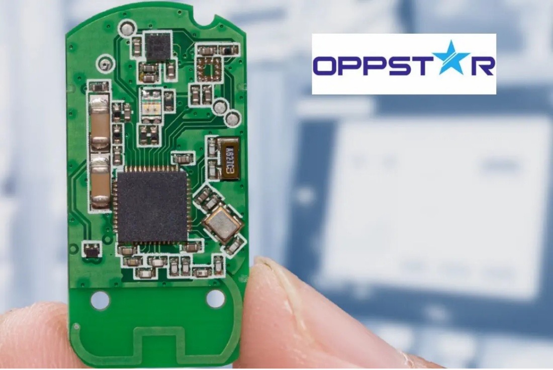
Figure 1. Oppstar’s ATI-based AIP board. (Source: Oppstar)
TAI’s work with railway customers gives the company field discipline. JR Kyushu has adopted TAI’s track inspection system for a cart that runs on rails used by Shinkansen high-speed trains. TAI has also shown Seaside-R6 in JR East-related demonstrations using cameras for railway operations and cost reduction. These deployments force the company to solve practical problems around weather, vibration, camera placement, maintenance, and false positives.
Japan’s labor shortage adds another reason for the push. Infrastructure inspection often depends on trained workers who know tracks, stations, factories, roads, and power lines. AI systems can help automate repetitive observation, flag anomalies, and reduce manual workloads. That does not make the chip a stand-alone answer. The value comes from the full package: cameras, sensors, models, hardware, software, deployment tuning, and customer workflow integration.
ISVs should watch the software stack closely. Reconfigurable silicon creates value only when development tools let application teams map models and update deployments without rebuilding everything by hand. Silicon teams should ask how TAI’s design flow handles model changes, sensor changes, quantization, verification, and long-term maintenance. CIOs should ask for evidence around uptime, power, latency, false alarms, field support, and replacement cycles.
The procurement lesson looks straightforward. Do not evaluate TAI against data center GPUs. Evaluate it against the cost of doing edge AI badly: cloud traffic, high latency, thermal failures, unreliable field boxes, site visits, missed detections, and hardware that never fits the environment. A mature-node reconfigurable chip can make sense when a fixed processor wastes power on logic the application does not need.
TAI still needs to prove the custom chip. Public materials do not disclose TOPS, memory bandwidth, package size, power envelope, throughput, or thermal design power. Those gaps matter for buyers. A credible evaluation should include benchmark sheets tied to the actual workload: object detection, image classification, video analytics, robotics control, sensor fusion, and railway safety monitoring under field temperature and vibration conditions.
TAI’s plan shows how edge AI hardware has started to specialize around physical environments. The company combines Seaside-R6, FPGA-based hardware experience, Sting Ray validation, a Manta Ray roadmap, and partners in Malaysia and Taiwan. If it can convert field experience into production silicon and usable software tools, TAI could give infrastructure buyers a practical way to move inference closer to sensors, reduce cloud dependence, and control heat and latency at the site.
What do we think?
TAI has picked a pragmatic silicon wedge. Reconfigurable edge inference fits railways, factories, robotics, and infrastructure because these sites need local decisions under power and heat limits. The 40 nm plan also fits cost and supply realities. The hard part comes next: production silicon, field software, repeatable deployments, and proof that customization does not slow every customer rollout in field trials.
Inflection signal
TAI’s roadmap may signal an inflection point in AI hardware outside the data center. Edge buyers now need inference where sensors collect data, not where cloud GPUs sit. That shifts value toward low-power silicon, mature nodes, reconfigurable architectures, and site-specific integration. If TAI and Oppstar commercialize the chip on schedule, the inflection point will appear first in infrastructure markets that need AI decisions at the physical edge. That change could reshape how CIOs budget physical AI deployments over time globally.
TAI joins the other 149 AIP companies in our AIP tracker service database. Normally, we wouldn’t include an FPGA-based device, but the Seaside is a purpose-built production chip, and we think it fits within the general description of an AIP. We also have a FPGA report in our AI library.
Take a look at our AI library, where, among things, we keep track of the 149 companies offering nearly 300 AI processors. JPR puts the “I” in AI (and because you will ask—Intelligence, market intelligence).
YOU LIKE THIS KIND OF STUFF? WE HAVE LOTS MORE. TELL YOUR FRIENDS, WE LOVE MEETING NEW PEOPLE.