
The UCIe Consortium released version 4.0 of its chiplet interconnect specification on November 12, 2026, extending the standard into memory connectivity and system management. The new UCIe.mem protocol promises up to 93.75% data efficiency and approximately 2.5 TB/s of bandwidth per millimeter of die edge. An optional power profile reduces link consumption by 30% to 80% under defined conditions. Security and reliability additions address multi-vendor packages and automotive systems. We examine the technology, commercial progress, and implications for future AI processors.
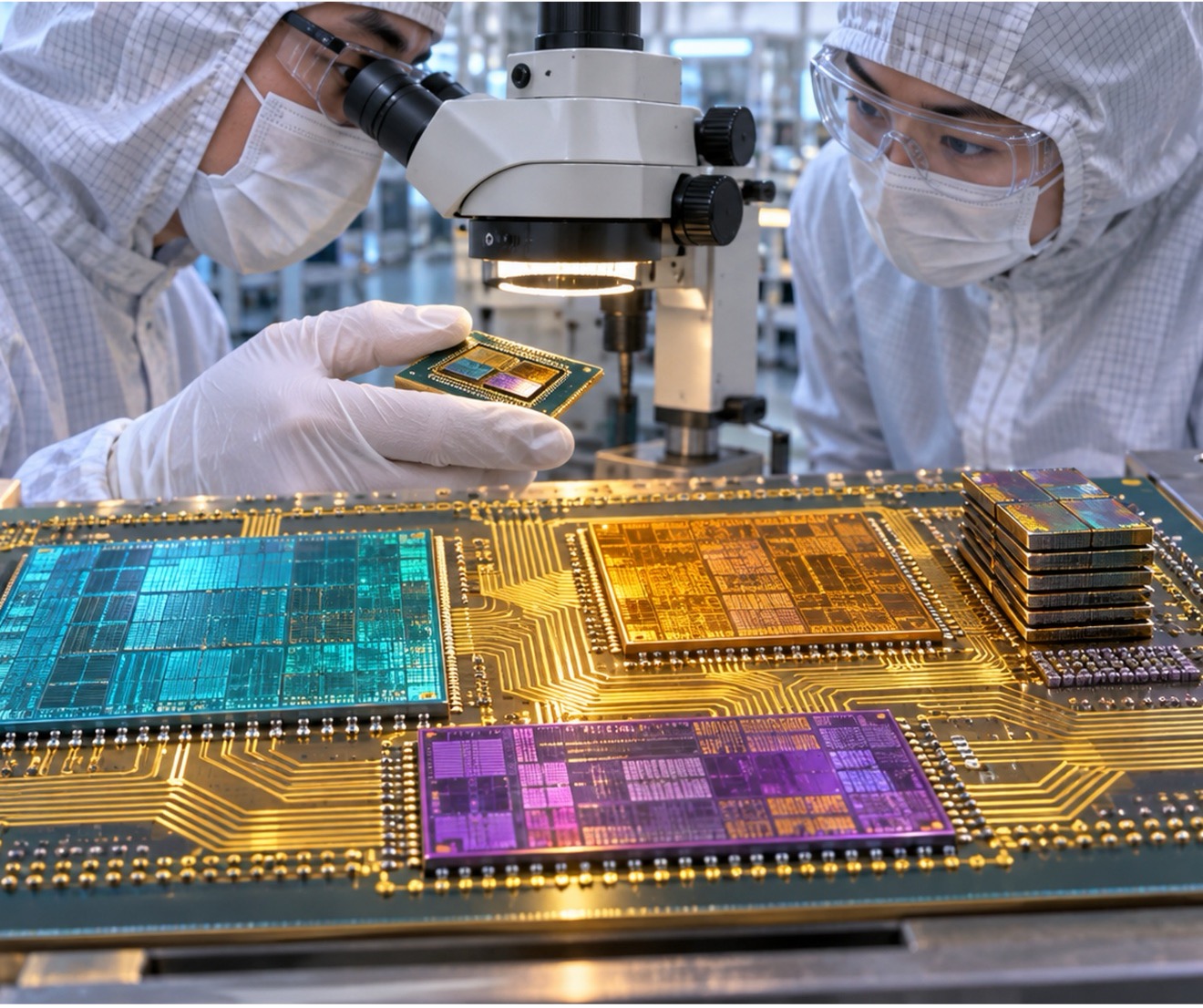
The Universal Chiplet Interconnect Express (UCIe) Consortium released Specification 4.0 on November 12, 2026, adding standardized memory connectivity, improved power efficiency, chiplet security, and automotive reliability features. The changes extend UCIe’s role from connecting individual dies to coordinating complete multi-chiplet systems.
The consortium began in March 2022 with 10 founding companies: Intel, AMD, Arm, ASE, Google Cloud, Meta, Microsoft, Qualcomm, Samsung, and TSMC. It incorporated in August 2022, adding Nvidia and Alibaba to its board. Membership subsequently exceeded 150 companies.
Debendra Das Sharma, an Intel senior distinguished engineer, chairs the consortium, and Samsung Corporate Vice President Cheolmin Park serves as president.
The organization collects membership dues, develops specifications, and supports interoperability. It sells no processors and reports no product revenue, unit shipments, or average selling prices. Its commercial influence depends on semiconductor companies incorporating the specifications into shipping products.
The consortium’s development history illustrates the expansion from basic die-to-die connectivity toward system integration.
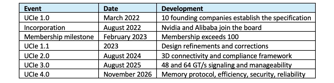
Table 1. UCIe specification milestones and consortium development. (Source: UCIe Consortium and industry reports)
Memory moves into the chiplet architecture
UCIe.mem introduces a standardized on-package connection between compute silicon and memory logic chiplets. The protocol separates memory control from the compute die, allowing designers to scale memory capacity and bandwidth independently of processor development.
A memory logic chiplet can manage HBM, LPDDR, or future memory technologies, and communicate with compute chiplets through existing UCIe physical interfaces and adapters.
The consortium reports up to 93.75% data efficiency and approximately 2.5 TB/s of bandwidth per millimeter of die edge. Ten millimeters of interface shoreline would theoretically support 25 TB/s at that density, although package geometry, controller capabilities, and memory technology determine usable bandwidth.

Figure 1. UCIe.mem connects compute chiplets to independent memory controllers.
UCIe.mem organizes memory requests and responses within 256-byte flits. Compact request and response slots reduce protocol overhead and improve link utilization.
Sharma identifies available die-edge space, commonly called shoreline, as a major constraint in advanced multi-die processors. Memory bandwidth requirements continue growing as AI models expand, particularly in inference systems that repeatedly retrieve model weights.
Standardized memory chiplets could allow memory suppliers to develop reusable controller designs and serve several processor vendors. Accelerator designers could increase capacity without redesigning their compute silicon.
Power efficiency and packaging density
UCIe 4.0 introduces an optional co-optimized power profile for UCIe-S and UCIe-A links. The consortium reports 30% to 80% lower link power at 64 GT/s under specified operating conditions.
The design uses quarter-data-rate signaling, direct sampling, adaptive voltage and termination, low-swing signaling, and improved timing tracking.
The savings require compatible die characteristics. Both devices should use similar process generations, share voltage rails, and maintain interconnect distances below approximately 5mm.

Figure 2. Chiplet power and interconnect.
Designers cannot assume the improvement applies to every heterogeneous package.
An enhanced bump map also increases UCIe-S bandwidth density by approximately 20% along the die shoreline and 10% per unit area at 48 and 64 GT/s.
These improvements address two expensive resources in advanced AI packages: physical interface space and the energy required to move data.
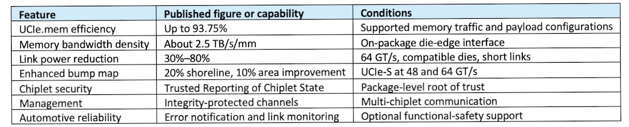
Table 2. UCIe 4.0 technical additions and operating conditions. (Source: UCIe Consortium 4.0)
The improvements in link power and bandwidth density depend on the physical relationship between chiplets. Short connections, compatible process technologies, and shared voltage rails allow designers to reduce signaling energy while increasing data throughput. Figure 2 illustrates the die-to-die connection through an interposer and the efficiency gains UCIe 4.0 targets.

Figure 3. UCIe 4.0 improves chiplet link power and bandwidth density.
These improvements give silicon teams more flexibility in allocating package power and die-edge bandwidth. Actual gains will depend on chiplet placement, process compatibility, and operating conditions. AI accelerator designers will need measured silicon results to determine how much of the theoretical improvement translates into system-level performance.
Security becomes a package-level requirement
Multi-vendor chiplet systems introduce security concerns that conventional monolithic processors can address within one design organization.
UCIe 4.0 adds Trusted Reporting of Chiplet State (TRoCs), allowing a package-level root of trust to query chiplet identity and operating state.
The specification also introduces bidirectional integrity-protected management channels and enhanced reset management.
These capabilities help system designers authenticate components, identify unexpected operating states, and coordinate initialization across several dies.
Automotive applications receive optional error notifications and link-health monitoring. Vehicle electronics developers can incorporate that information into functional-safety systems and long-term reliability monitoring.
Honda R&D and Mirise Technologies have expressed support for the automotive additions.
UCIe joins an increasingly complex interconnect environment
Modern processors and AI systems use several interconnect technologies because communication requirements change across the system hierarchy.
On-die fabrics move transactions among processor blocks. Die-to-die interfaces connect chiplets inside packages. Scale-up networks connect accelerators, while scale-out networks connect servers and racks.
UCIe addresses the package-level portion of that hierarchy.

Table 3. Interconnect technologies and their principal applications. (Source: Specifications and documentation)
Cadence’s Arif Khan expects designers to combine standardized interfaces with specialized fabrics at different levels. Axiomise CEO Ashish Darbari identifies verification across protocol boundaries as a continuing engineering challenge.
Interoperability requires compatible implementations, validation tools, and consistent management behavior across suppliers.
Commercial adoption determines the outcome
The consortium has demonstrated progress through member silicon and product announcements.
Intel and Synopsys demonstrated the Pike Creek cross-foundry test chip in 2023. GUC announced a UCIe PHY implementation on TSMC N3P in March 2025, reporting 32 Gb/s per lane. Rebellions identifies its Rebel-Quad NPU as a UCIe-Advanced implementation.
AMD has outlined native UCIe 1.1 connectivity for its Versal RF-series adaptive SoCs, with production chiplets expected in late 2027.
These examples demonstrate engineering activity across foundries, IP suppliers, and processor developers. They do not establish commercial deployment of UCIe 4.0 memory links.
Silicon teams should evaluate UCIe.mem against existing HBM and LPDDR interfaces, confirm partner PHY support, and measure actual link power and bandwidth. ISVs should monitor how future memory configurations affect model capacity and inference throughput. CIOs should ask suppliers about interoperability, security attestation, and product availability.
UCIe 4.0 establishes a common technical foundation for memory expansion and multi-vendor chiplet integration. The next evidence will come from validated silicon, interoperable memory controllers, and commercial products that demonstrate the specification’s efficiency claims under production workloads.
What do we think?
UCIe 4.0 addresses several practical constraints in advanced packaging: memory bandwidth, shoreline, power consumption, and chiplet security. The memory protocol could help AI processor designers scale capacity independently of compute. We want measured silicon results, interoperability testing, and production commitments before assigning commercial value to the efficiency claims. Specification adoption matters when products reach customers and demonstrate measurable improvements.
Inflection point. UCIe 4.0 does not create an inflection point in AI hardware today. The specification provides a technical path toward one by standardizing memory connections across chiplets from different suppliers. An inflection point would require production memory logic chiplets, interoperable PHYs, verified power savings, and broad adoption among accelerator developers. Existing demonstrations and announced roadmaps establish early momentum. Watch for 2027 and 2028 silicon announcements, compliance results, and customer deployments. Those developments will determine whether standardized memory chiplets change AI processor economics and system design.
UCIe 4.0 carries particular significance for AI processor development, where memory bandwidth, data movement, and power consumption increasingly constrain performance. Standardized memory chiplet interfaces could allow designers to scale compute and memory independently, combine silicon from multiple suppliers, and reduce development costs. If the industry adopts UCIe.mem broadly, it could reshape AI accelerator architectures and improve the economics of future AI systems.
WHAT DO YOU THINK? GOOD ENOUGH TO TELL YOUR FRIENDS ABOUT IT? YOU HAVE OUR PERMISSION TO SHARE IT.