
Evaluating a new AI architecture usually starts with a wait: specialized boards, custom tooling, an NDA. BrainChip just deleted that step. Its AKD1500 PCIe card drops into any desktop, workstation, or industrial PC and runs your models on your streaming data during that afternoon. The same model then runs unchanged on an M.2 module, packaged silicon, or licensed IP. Patent filings across the industry say the architecture behind it sits exactly where the invention money is going right now.
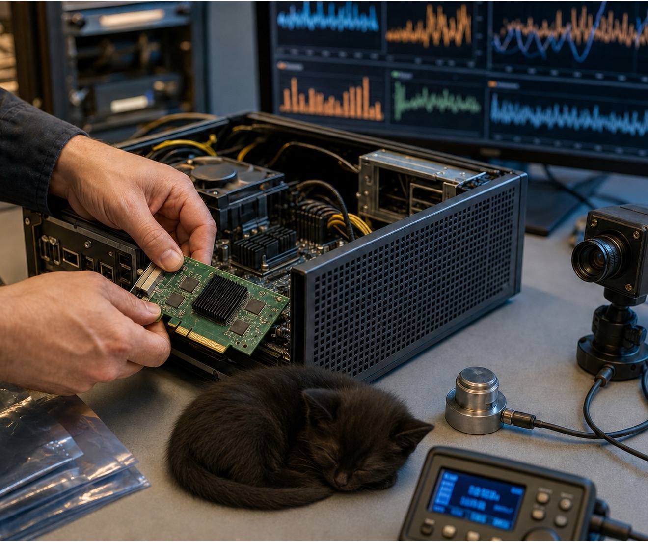
BrainChip put its AKD1500 edge AI coprocessor on a PCIe development card that installs in a standard slot in a desktop, workstation, industrial PC, or single-board computer. The card runs models built in existing frameworks against a team’s own streaming data, and it sells through the company’s online store with open tools and a model library, no subscription and no license fee.
The card matters less than the list it completes. Akida now ships as an evaluation card, an M.2 module, packaged and unpackaged silicon, and IP that a chip team can license into its own SoC. A model validated on the card runs on the deployed part without changes, so evaluation and productization stop competing for the same calendar.

Table 1. Akida ships in five forms, one toolchain throughout. (Source: BrainChip)
“The first challenge in evaluating new AI architectures is getting your hands on silicon and tools,” said Steve Brightfield, BrainChip’s chief product officer. “If you have a PC with a spare slot, you can be running your own models on Akida this afternoon.”
CEO Sean Hehir frames the same point as a roadmap: card to IP, one adoption path.
Why the memory question decides the design
AKD1500 runs 32 neural processor units on a 22nm FD-SOI digital process with 100K of SRAM per NPU, 1 MB of local on-chip memory, and 1 MB of dual-port memory. It reaches 800 effective GOPS under 1 mW per GOPS, draws about 200 mW over PCIe, and clocks from 5 to 400 MHz. Models come in through TensorFlow, Keras, and PyTorch APIs, and the part learns on device without a cloud connection.
The number that explains the power figure sits in the memory line. BrainChip sizes the fabric so an entire network fits inside it, which removes most of the weight traffic to and from DRAM. Event-based execution then skips the zero activations. Data movement dominates the energy budget in edge inference, so a design that keeps weights and activations next to the multipliers wins on joules per inference before anyone counts multipliers. The company taped the part out in GlobalFoundries’ 22nm FD-SOI for the leakage characteristics that let an always-on sensor design run on a battery.
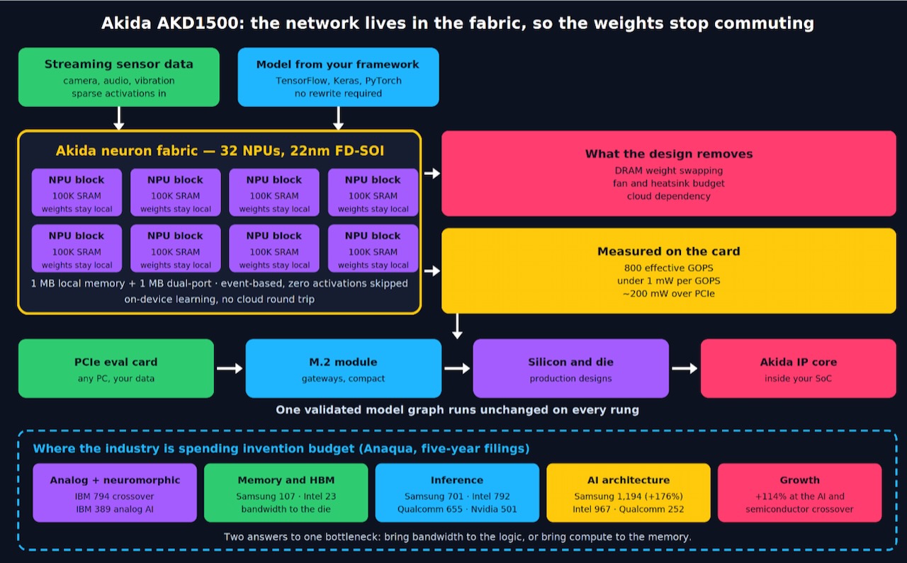
Figure 1. Akida keeps weights in fabric; patent filings back memory-near-compute.
That design choice reads as a niche position until you look at what the rest of the industry patents.
The patent record points in the same direction
Anaqua’s 2026 semiconductor patent study measures where companies spend invention budgets. Filings at the AI and semiconductor intersection grew 114% over five years against 78% for the broader sector, and inference leads every subcategory. Toni Nijm, Anaqua’s chief product officer, ties that to the shift from training models to running them at higher efficiency, and has stated this intersection carries the largest growth inside the industry.
Look at which subcategories absorb the filings, and the pattern gets specific. IBM holds 794 AI-semiconductor crossover filings and 389 in analog AI, built on phase-change memory and the Spyre accelerator, all aimed at the von Neumann bottleneck. Samsung turns memory expertise into 1,194 architecture filings, first place in HBM with 107, second in inference with 701, and second in analog AI. Intel sits second in AI-in-IC architecture with 967, and eighth in inference with 792. Nvidia, which owns the data center, ranks seventh in GPU-titled filings with 49 and 15th in inference with 501, because CUDA carries that position, and patent volume plays a supporting role.

Table 2. Filings cluster where compute moves toward memory. (Source: Anaqua 2026 semiconductor patent report)
Two answers to one problem show up across those rows. Large-system vendors move bandwidth toward the die with HBM. Analog and event-based designers move compute toward the memory. BrainChip sits in the second group with a digital implementation, which gives it standard tooling and no analog calibration burden. Chinese state-affiliated institutes filed 5,387 inference and accelerator patents over the same five years, roughly triple Samsung’s 1,897, so expect this class of design to attract more entrants.
Volume lives at the edge
Timing works in BrainChip’s favor. ABI Research puts the edge AI chipset market at $34.4 billion in 2026, reaching $96 billion by 2031, with unit shipments rising from 711 million to 1.59 billion.

Table 3. Edge AI chipsets nearly triple by 2031. (Source: ABI Research, 2Q 2026 market update)
Industrial sensors, cameras, robots, and wearables set the requirements for that spend: a fraction of a watt, no fan, no cloud dependency, and personalization after deployment. Every one of those constraints points back at where the weights live.
What to measure on the card
Teams running an evaluation should treat the card as a power meter with a PCIe connector. Load the production model, stream real sensor data through it, and log joules per inference and end-to-end latency against the current part. Activation sparsity in the incoming datasets how much the event-based fabric saves, so synthetic benchmarks understate the result on camera and vibration workloads and overstate it on dense inputs. Users should check how much of the network fits in the 1 MB of local memory, since a model that spills starts paying DRAM energy again. They should also exercise the on-device learning path with a personalization case, because that capability changes the retraining pipeline and the privacy story at the same time. BrainChip sells the rest of the line for whatever comes next: M.2 modules, NICLA and Arduino boards, silicon, die, and IP cores.
For silicon teams, the useful test now costs the price of a card and an afternoon to load their model, stream their data, measure joules per inference against their current part, then decide whether the IP belongs in their next SoC. For CIOs, the same logic applies one level up, because a fleet that learns locally changes the bandwidth and privacy math. The patent record says the memory-near-compute approach keeps drawing investment, and BrainChip removed the last excuse for not testing it.
What do we think?
The product news is a distribution decision, and distribution decides adoption for new architectures. Every rung from card to IP core runs the same model graph, which turns a six-month evaluation into an afternoon. The technical claim underneath holds up: keep the network in fabric and skip zero activations, and the power numbers follow. Users should ask BrainChip for joules per inference on their workload, not GOPS.
Inflection point. The direction of the filings matters more than the totals. Inference leads every subcategory, analog and neuromorphic work draws sustained investment from IBM and Samsung, and memory bandwidth absorbs the rest, which marks an inflection point away from transistor count as the lever. Low-cost evaluation hardware accelerates that turn because architectures spread once engineers measure them on their own data. Edge units more than doubling to 1.59 billion by 2031 gives the shift its volume.
YOU LIKE THIS KIND OF STUFF? WE HAVE LOTS MORE. TELL YOUR FRIENDS, WE LOVE MEETING NEW PEOPLE.