
Three chipmakers now chase the same bottleneck from three different directions. Qualcomm bonds compute directly onto memory with its High Bandwidth Compute architecture. Micron spreads compute and memory across a tiered hierarchy built on SOCAMM modules and the LPDDR6 roadmap. Intel, absent from mainstream memory production for decades, studies a third path built around packaging technology, not DRAM production itself.

Three architectures, one bottleneck
AI accelerators shuttle enormous tensors between processing units and memory on every pass. Arithmetic throughput has outpaced off-chip bandwidth for years, and that gap now stalls many workloads on data delivery, not raw computation. High-bandwidth memory closes part of that gap: It bonds thinned DRAM dies into a vertical stack, links them through thousands of through-silicon vias (TSVs), and connects the stack to a processor over an interface thousands of bits wide, trading some capacity and thermal headroom for far higher bandwidth and lower energy per bit than planar DDR memory delivers. That trade defines the ground Qualcomm, Micron, and now Intel compete on.
A packaging comeback, not a DRAM comeback
Intel began as a memory company in 1968, when Robert Noyce and Gordon Moore left Fairchild Semiconductor to start it, and SRAM and DRAM chips carried the business until Japanese competition and shrinking margins pushed Intel toward microprocessors in the 1980s. Later, storage efforts followed a similar arc. Intel sold its NAND flash and SSD unit to SK Hynix in 2020, and that business became Solidigm. Intel then discontinued its Optane line, built on 3D XPoint technology, in 2022, and took a $559 million inventory impairment after adoption stalled. Re-entering conventional DDR DRAM or NAND production today would pit Intel against Samsung, SK Hynix, and Micron, three companies that already hold specialized process technology, large fabrication capacity, and entrenched customer relationships. Chief executive Lip-Bu Tan points Intel somewhere else: the boundary where compute, memory, and advanced packaging meet.
The stacking options on the table
Tan named memory architecture one of his pet projects in August 2026 and said stacking memory directly onto a CPU “could make a lot of sense,” adding that “there’s a lot of new technology” emerging in the space. Several approaches could satisfy that ambition: placing HBM stacks beside compute tiles, bonding cache or memory dies above logic, or building dedicated embedded-memory chiplets. Each option shortens interconnects, cuts capacitance, and opens thousands of parallel signal paths, and each carries a matching cost. Memory sitting directly above hot CPU or accelerator cores hits thermal ceilings fast, stacked dies complicate yield, testing, and repair, and logic and DRAM favor different fabrication processes that make bonded separate dies a more practical route than one monolithic die carrying both. Tan has also disclosed an XBM patent that removes HBM’s silicon interposer entirely and uses Universal Chiplet Interconnect Express to bond memory directly onto a CPU, with commercialization targeted for sometime after 2030.
The technology Intel already has
Intel does not start from zero on packaging.
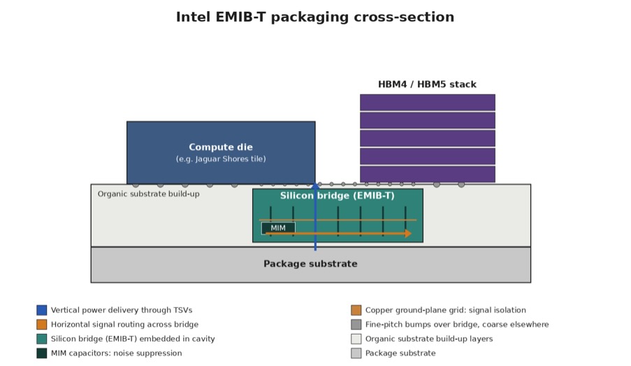
Figure 1. Block diagram of Intel EMIB-T memory.
Foveros Direct uses fine-pitch hybrid bonding to stack dies vertically, and Intel’s forthcoming 18A-PT process connects to a top die at an interconnect pitch under 5 micrometers. EMIB-T complements that stack: It embeds silicon bridges carrying TSVs inside the package substrate, routes power vertically through the bridge itself, and connects logic to HBM3, HBM3E, and HBM4 stacks without a full-size silicon interposer. Together, the two technologies could let Intel assemble complete compute-memory packages even when a separate manufacturer supplies the DRAM dies inside them.
Credibility without commitment
Intel backed the technical case with a personnel move: It hired Seok-Hee Lee, the former chief executive of SK Hynix, as executive vice president of Intel Foundry, placing him over advanced packaging, system integration, and back-end manufacturing. The hire lends the exploration real credibility. It does not amount to a commitment: Intel has announced no product, no fabrication plan, and no commercial timetable. A full return to memory manufacturing would cost billions of dollars, demand years of process development, and pull qualification cycles away from Intel’s processor roadmap and its foundry expansion.
The likelier outcome sits short of a commodity-memory revival. Intel could ship differentiated cache, stacked-memory, or packaging products that raise effective bandwidth for AI systems, co-design memory interfaces alongside CPUs and accelerators, manufacture selected logic or controller dies itself, and integrate third-party HBM through EMIB or Foveros. That path separates Intel from Qualcomm’s single stacked-package bet and from Micron’s JEDEC-standardized tiering—Intel positions itself as the packaging layer connecting other companies’ memory and compute, not as a competitor selling commodity bits.
For silicon teams and ISVs building against next-generation accelerators, Intel’s packaging roadmap marks where interconnect standards and thermal budgets head next. For CIOs and IT buyers, it marks a shift already underway; packaging technology, not raw DRAM capacity, increasingly sets the ceiling on system performance and total cost of ownership, and memory sourcing decisions will keep moving with it.
Intel’s prospective comeback amounts to a systems-engineering wager, not a memory-manufacturing one. AI hardware performance now turns on data supply as much as arithmetic capacity, and the platform that keeps its compute units fed carries the advantage. Turning packaging, interconnect, and memory architecture into one optimized system could put memory back at the center of Intel’s identity, on different terms from the commodity fight that pushed the company out decades ago.
Qualcomm, Micron, and Intel each stake out a distinct architecture bet on memory: a stacked package, a tiered hierarchy, and a packaging layer connecting other companies’ silicon. Rambus, Infineon, and Everspin extend that hierarchy from the supply side, building the chipsets, flash, and MRAM tiers Micron’s approach depends on. The wider group signals how far the shift has spread; the three architecture bets signal where the real strategic decisions get made.
What do we think?
Intel’s memory comments read as exploration, not commitment, and that distinction matters. Qualcomm and Micron already ship products built on their memory bets; Intel still weighs patents, hires, and packaging roadmaps. The Seok-Hee Lee hire and the XBM patent add technical weight to the idea. A shipped product sits years away and depends on capital, ecosystem support, and Intel’s willingness to prioritize memory over its processor and foundry commitments.
Inflection point. Three major chipmakers converging on memory architecture at the same time marks an inflection point in AI infrastructure. Data movement, not raw arithmetic, now sets the ceiling on system performance, and Intel’s willingness to reconsider a business it exited decades ago shows how far that shift has traveled. Whether or not Intel ships a product, the exploration itself confirms that memory placement has become a competitive battleground central to the next phase of AI hardware.
LIKE WHAT YOU’RE READING? TELL YOUR FRIENDS; WE DO THIS EVERY DAY, ALL DAY.