
AI infrastructure runs into one shared problem: Moving data now costs more than computing it. Qualcomm and Micron each built an answer, aimed at opposite ends of the same bottleneck. Qualcomm’s High Bandwidth Compute (HBC) architecture stacks compute directly onto memory in a single package. Micron keeps compute and memory as separate components and spreads the job across a wider hierarchy of memory tiers, joined by Rambus, Infineon, and Everspin. Both bets share the same premise: Memory now decides AI performance as much as compute does.
Qualcomm pursues its High Bandwidth Compute (HBC) architecture by stacking a logic die directly beneath an LPDDR package through dense through-silicon vias and erasing the boundary between compute and memory. Micron pursues a different idea: keep compute and memory as separate components and spread the job across a wider hierarchy of memory tiers instead, sized for cost, power, and latency. Rambus, Infineon, and Everspin each supply pieces of that hierarchy, betting that AI’s growing appetite is a multi-technology problem, not a single-package one.
Money and supply back Micron’s bet. HBM demand outstrips supply as AI accelerators consume every gigabyte producers can stack, pushing engineers to redirect memory technologies built for smartphones into the data center. Low-power DRAM (LPDDR) and the Small Outline Compression Attached Memory Module (SOCAMM) compete for a role in AI racks as performance per watt becomes a core metric, reshaping purchasing math for ISVs, silicon teams, and CIOs alike.
Micron builds a wider hierarchy
Smartphone makers built LPDDR for battery-powered devices, prizing low power draw and compact size, and those same traits now draw AI data centers toward it. JEDEC’s upcoming LPDDR6 update extends the standard beyond mobile platforms to cover accelerated-computing workloads. The SOCAMM form factor pairs with LPDDR to deliver higher capacity and energy efficiency near the CPU, narrowing the memory wall for token-heavy models and drawing roughly one-third the power of a standard DDR5 RDIMM. Where Qualcomm’s HBC changes the package, SOCAMM changes the module and the socket, and leaves the CPU-memory boundary untouched.
Micron’s recently launched 256GB SOCAMM targets dense, serviceable server builds and gives systems far more memory per CPU than traditional RDIMMs support, running on Micron’s 1-gamma DRAM process and monolithic 32Gb dies to cut time-to-first-token latency by off-loading KV-cache from HBM.
Micron’s 256GB SOCAMM targets dense, serviceable server builds and gives systems far more memory per CPU than traditional RDIMMs support. (Source: Micron)
Low-power DRAM has a real opening in the data center right now. Micron sees application spaces genuinely well suited to the feature set this product delivers. AI workloads keep shifting toward inference, where response time and memory footprint sit at the center of the design problem. Memory bandwidth matters enormously in that situation.
Same pressure, opposite bets
Qualcomm, on the other hand, reports up to 6× higher bandwidth per watt than traditional HBM delivers, a gain it achieves by removing the chip-boundary crossing entirely. Qualcomm concentrates that bet in a single stacked package built for one accelerator family, measuring success in bandwidth-per-watt multiples: 133 TB/s of effective bandwidth per card on the Dragonfly AI250 today, and a targeted 54× increase over the AI200 baseline once HBC Gen 2 ships on the AI300, aimed at fiscal 2027 commercialization.
Micron spreads its bet across JEDEC-standardized hardware that multiple vendors already ship, and sells into any server platform that adopts the SOCAMM standard today. Qualcomm concentrates risk and reward in one execution timeline running toward a single future product generation. Micron distributes both across a hierarchy that server builders can adopt piece by piece, starting now.
Why HBM alone falls short
Micron doesn’t position SOCAMM as an HBM replacement, and neither company claims its architecture eliminates HBM. It sits in the middle of a broader hierarchy: hot KV cache stays in HBM, warm KV cache stays in low-power DRAM, and cold KV cache goes to fast storage.
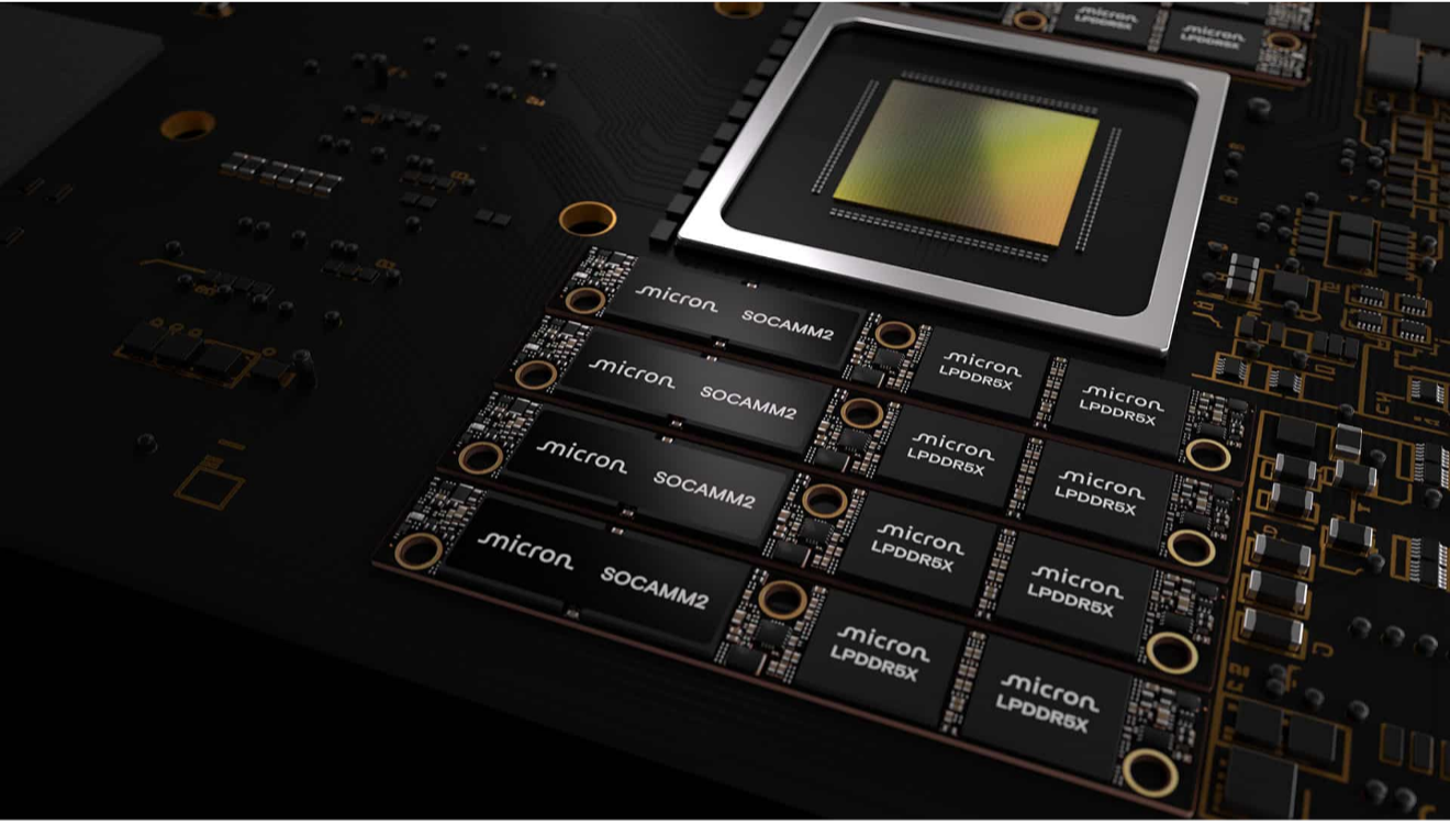
Figure 1. Micron’s SOCAMM HBM replacement. (Source: Micron)
LPDDR and SOCAMM gain traction for capacity and fast access time, not because chipmakers built them for AI. AI demand keeps HBM fully committed : The HBM is spoken for because of AI, and that pressures DRAM. Hyperscalers pay for efficiency because they run the numbers on electricity and system cost, the same math justifying Qualcomm’s stacked-package premium for workloads fitting its narrower target.
Rambus and Infineon extend the hierarchy Qualcomm skips
Rambus recently announced its LPDDR-based SOCAMM2 chipset, the first in a planned family of server module chipsets for AI systems, adding a second supplier to the tier Qualcomm’s design bypasses entirely. Inference tells a different story than training, Rambus points out, citing lower-cost options such as GDDR and DDR that often meet the need. GPUs spend more than half their power moving data to memory, Steven Woo, Fellow and Distinguished Inventor at Rambus, said, driving attention toward interconnects such as CXL—a software-defined pooling layer with no equivalent in Qualcomm’s single-package design.
Infineon Technologies believes the AI stack needs multiple device-class tiers to balance cost, power, and persistence: HBM at the top, SRAM for latency-sensitive work, and DRAM, CXL pooled memory, and flash SSDs for context retention and model storage.

Figure 2. Infineon doesn’t think one size fits all. (Source: Infineon)
Infineon sees NOR flash as an overlooked enabler, noting Nvidia’s GB200 racks carry it for boot code and as a hardware security anchor storing keys and certificates, a role no amount of near-memory compute replaces. Infineon believes the AI stack needs multiple memory device-class tiers addressing cost, power, and persistence.
MRAM claims a role Qualcomm’s design doesn’t reach
NOR flash faces competition from MRAM for code, firmware, and persistent state, a tier that sits outside Qualcomm’s HBC scope entirely. As AI spreads outward, the data center, network, and edge all need persistent memory support, and discrete MRAM eases data center bottlenecks by letting systems run more inference locally. Everspin’s new UNISYST MRAM unifies code storage and data memory in one non-volatile architecture for edge AI and industrial designs, cutting FPGA code-writing time to seconds versus the 10 to 20 minutes NOR flash requires.
Two philosophies, one problem
Rack designers face a choice: concentrate compute-memory risk in one package or spread it across proven standards. CXL pooling powers that path, cutting stranded capacity and pulling power off pin-dense interfaces so engineers pin latency-critical data to local DRAM and off-load heavy datasets to a shared pool. Qualcomm picks the first path, stacking compute and memory into one leap that erases the boundary for a single accelerator line. Micron, Rambus, Infineon, and Everspin pick the second, drawing on JEDEC standards, CXL, and DIMM sockets, spanning HBM, LPDDR, DDR, NOR, and MRAM across four suppliers.
Neither camp claims a final answer. Qualcomm’s stacked package targets peak efficiency for one accelerator line and carries the execution risk of a single roadmap running toward 2027. Micron, Rambus, Infineon, and Everspin bet on breadth: a hierarchy that lets any server builder mix memory types to fit a workload’s cost, power, and latency budget today. Both bets share one premise—memory now decides AI performance and economics as much as compute does, and the industry’s next round of gains comes from how well engineers place data.
What do we think?
Qualcomm’s HBC concentrates risk in one packaging bet with a bigger potential payoff two fiscal years out. Micron’s tiering strategy spreads risk across four vendors and existing JEDEC standards, giving buyers optionality today. Both responses confirm the same diagnosis: Data movement, not raw arithmetic, now sets the limit on AI system performance and cost.
Inflection point. Memory diversification marks an inflection point in AI infrastructure. The industry stopped treating memory as one commodity and started treating it as a portfolio of specialized tiers, each tuned to a workload. Qualcomm’s HBC bets that packaging integration marks its own inflection point in how memory and compute connect. Together, the two signals point toward an industry-wide reset: Buyers weigh memory-hierarchy design and packaging innovation equally, and total energy per token replaces peak bandwidth as the top purchasing metric.
Qualcomm, Micron, Rambus, Infineon, and now Intel are looking over the fence at memory.
LIKE WHAT YOU SAW HERE? SHARE THE EXPERIENCE, TELL YOUR FRIENDS.